HomeTag

High-Speed PCB Design - KKPCB

Microvia PCB: High-Density Interconnect Solutions for Advanced Electronics

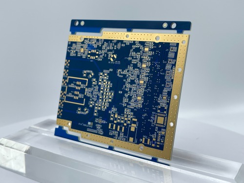
Microvia PCB: High-Density Interconnect Solutions for Advanced Electronics As electronic devices become smaller, faster, and more complex, designers face increasing challenges in routing high-density circuits. Microvia PCB technology provides a solution by enabling high-density interconnects (HDI), allowing for compact multilayer designs with superior electrical performance. A Microvia PCB uses extremely small vias, typically less than...
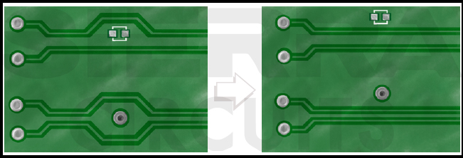
Differential Pair PCB: Design Guidelines for High-Speed Signal Integrity

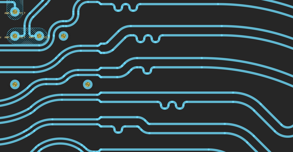
Differential Pair PCB: Design Guidelines for High-Speed Signal Integrity In modern high-speed digital systems, Differential Pair PCB routing has become a fundamental design technique for maintaining signal integrity and reducing electromagnetic interference. Interfaces such as USB, HDMI, PCIe, Ethernet, and high-speed SerDes rely heavily on differential signaling to achieve reliable high-speed data transmission. A well-designed...

Key Manufacturing Factors That Affect Controlled Impedance PCB Accuracy

Key Manufacturing Factors That Affect Controlled Impedance PCB Accuracy In today’s high-speed electronics market, Controlled Impedance PCB manufacturing has become a fundamental requirement for ensuring excellent signal integrity and stable electrical performance. As operating frequencies and data transmission speeds continue to rise, even minor impedance deviations in a controlled impedance PCB can result in signal...

Designing Buried Via PCBs for High-Density Routing and Signal Integrity Optimization

As electronic systems continue to evolve toward higher speeds, smaller form factors, and increased functionality, traditional through-hole via structures are becoming a limiting factor. Buried Via PCB technology has emerged as a key solution for achieving high-density routing and optimizing signal integrity, especially in HDI, high-speed digital, and RF designs. By embedding vias between internal...

High Speed PCB Engineering Strategies for Ultra-Reliable, High-Bandwidth, Next-Generation Electronic Systems

A High Speed PCB is no longer a specialty board reserved for telecom giants—it has become the core platform for every high-bandwidth, low-latency, high-frequency electronic architecture. Whether powering 56G/112G SerDes, PCIe 5.0/6.0 interconnects, next-generation routers, AI accelerator hardware, or advanced radar/5G infrastructure, the High Speed PCB defines the system’s ultimate signal integrity, timing accuracy, power...

Impedance Matching in HDI PCB Design

In modern HDI PCB design (High-Density Interconnect PCB design), achieving precise impedance matching is essential for maintaining signal integrity, minimizing reflection, and ensuring high-speed signal transmission. As data rates increase and circuit density grows, impedance control in HDI PCB layout becomes more complex due to fine trace geometries, microvias, and multilayer stack-ups. Effective impedance matching...

Optimizing High-Frequency Stability and Low-Loss Transmission Using RF-35 PCB Laminates for Modern Wireless Systems

As modern wireless systems continue to evolve toward higher frequencies and faster data rates, achieving high-frequency stability and low-loss signal transmission has become a critical requirement in RF PCB design. One of the most effective ways to optimize high-frequency PCB performance is through advanced material selection—specifically RF-35 PCB laminates. RF-35 laminates are engineered for high-frequency...

PTFE PCB Explained: Properties, Advantages, Applications & Comparison with FR4

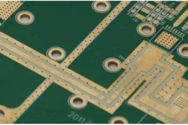
Understanding PTFE PCB: A Comprehensive Technical Overview Printed circuit boards (PCBs) form the backbone of modern electronic systems. While FR4 remains the industry standard for general-purpose PCB manufacturing, PTFE PCBs occupy a special place in high-performance, high-frequency, and harsh-environment applications. This guide provides an in-depth exploration of PTFE PCB technology—its material properties, technical specifications, differences...

RO4350B PCB Hybrid Stackup Design and Lamination Challenges in Mass Production

As high-frequency PCB design becomes increasingly prevalent in RF, 5G, and high-speed digital systems, the use of RO4350B PCB materials in combination with standard FR4 has led to the widespread adoption of hybrid PCB stackup design. A RO4350B hybrid stackup PCB enables designers to balance cost efficiency and high-frequency performance, making it ideal for complex...

What is Backdrill and How Was It Done in PCB Manufacturing?

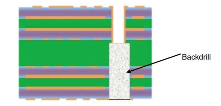
As electronic products continue to demand higher data rates, faster signal transmission, and improved signal integrity, traditional PCB manufacturing methods face increasing challenges. In high-speed PCB designs, even small parasitic effects caused by vias can negatively impact signal performance. One common issue is the via stub, which is the unused portion of a plated through...