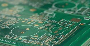
As electronic systems continue to evolve toward higher speeds, smaller form factors, and increased functionality, traditional through-hole via structures are becoming a limiting factor. Buried Via PCB technology has emerged as a key solution for achieving high-density routing and optimizing signal integrity, especially in HDI, high-speed digital, and RF designs.
By embedding vias between internal layers instead of extending them through the entire board, buried via PCBs significantly improve routing efficiency while minimizing electrical discontinuities.
What Is a Buried Via PCB?
A buried via PCB is a multilayer circuit board in which vias connect only internal layers and are not visible on the outer surfaces. These vias are formed during intermediate lamination stages, making them completely enclosed within the PCB stackup.
This structure allows designers to:
- Preserve outer layers for component routing
- Improve layout flexibility
- Maintain clean surface topology for fine-pitch components
Why Buried Via PCBs Enable High-Density Routing
Maximizing Available Routing Channels
In modern PCB designs, especially HDI layouts, routing space is extremely limited. Buried vias eliminate unnecessary via pads on outer layers, freeing up valuable space for:
- High-speed differential pairs
- Dense BGA fan-out
- Power and ground routing
This directly improves routing efficiency and reduces overall board size.
Reducing Via Congestion in Critical Areas
Buried vias can be strategically placed between specific internal layers, allowing designers to:
- Isolate dense routing regions
- Avoid congestion near sensitive signals
- Improve layout organization
This is particularly important in high-speed and RF designs, where excessive via density can lead to signal interference and impedance disruption.
Signal Integrity Advantages of Buried Via PCB Design
Minimized Via Stub Effects
Traditional through vias often create unused conductive stubs, which behave like resonant structures at high frequencies. These stubs can introduce:
- Signal reflections
- Insertion loss
- Phase distortion
Buried vias eliminate unnecessary via length, resulting in:
- Reduced reflection
- Cleaner signal transmission
- Improved eye diagram performance
Improved Impedance Control
Buried via structures provide better control over impedance because:
- Via length is precisely defined
- Dielectric environments are more stable
- Signal paths are shorter and more direct
This is critical for applications requiring strict impedance control, such as:
- High-speed serial communication
- RF circuits
- High-performance computing systems
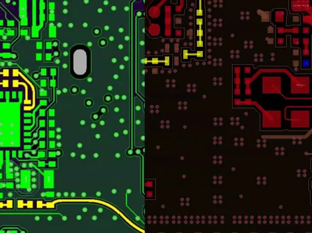
Buried Via PCB Stackup Design Considerations
Layer Pair Planning
Effective buried via PCB design begins with proper stackup planning. Designers must determine:
- Which layers require interconnection
- Placement of power and ground planes
- Lamination sequence for via formation
Well-planned layer pairing ensures both electrical performance and manufacturability.
Balancing Performance and Manufacturability
While buried via PCBs offer clear electrical advantages, they also introduce additional complexity, including:
- Multiple lamination cycles
- Increased drilling steps
- Higher fabrication costs
Designers must balance:
- Signal integrity requirements
- Board thickness constraints
- Production yield and cost
Early collaboration with PCB manufacturers is essential.
Manufacturing Challenges in Buried Via PCBs
Producing buried via PCBs requires advanced process control, including:
- Accurate sequential lamination
- Precise drilling and registration
- Uniform copper plating
- Tight layer-to-layer alignment
Any deviation in these processes can affect both electrical performance and reliability.
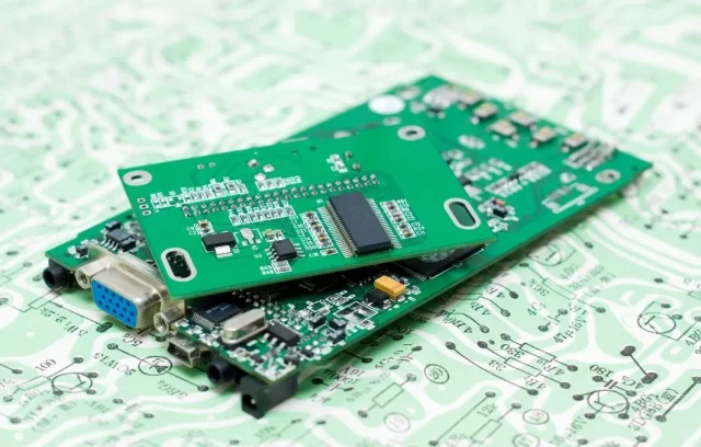
Typical Applications of Buried Via PCB Technology
Buried via PCBs are widely used in applications where both density and performance are critical:
- HDI consumer electronics
- High-speed networking equipment
- RF and microwave modules
- Industrial automation systems
- Aerospace and defense electronics
These applications benefit from compact layouts without compromising signal quality.
Conclusion
Buried via PCB technology is no longer optional in advanced electronic design—it is essential. By enabling high-density routing, reducing signal degradation, and improving impedance control, buried via PCBs play a crucial role in modern high-speed and high-performance systems.
With proper stackup planning and close coordination with manufacturers, engineers can fully leverage buried via technology to achieve optimal performance, reliability, and scalability in next-generation PCB designs.
