HomeTag

High Density Interconnect - KKPCB

Blind & Buried Vias in HDI PCB: Design & Manufacturing Expertise

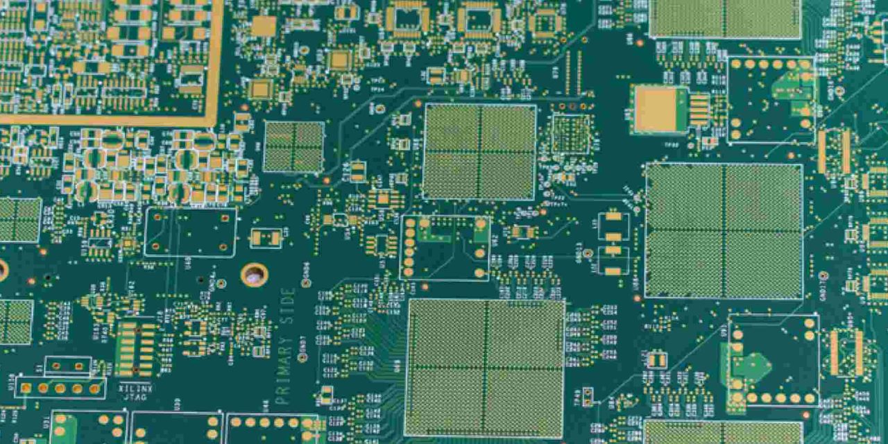
Blind and Buried Vias in HDI PCB Design: Engineering Principles, Manufacturing Constraints, and KKPCB’s Advanced Capabilities As high-density interconnect (HDI) technology becomes essential in 5G, wearables, automotive radar, aerospace, and compact IoT systems, PCB designers increasingly rely on blind vias and buried vias to meet aggressive space, performance, and reliability requirements. These via structures allow...
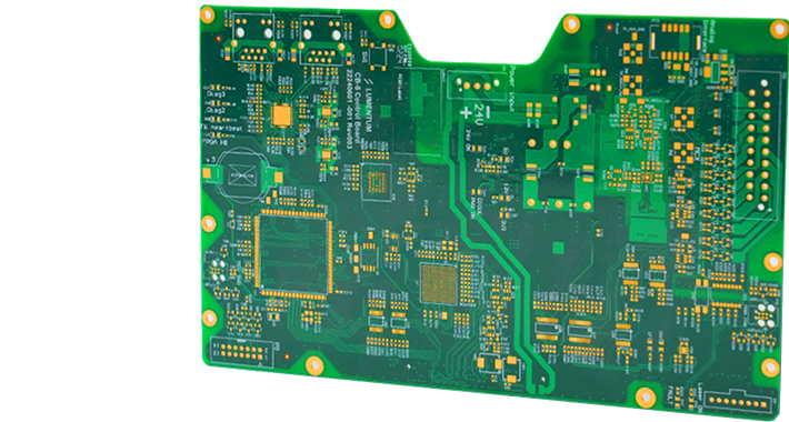
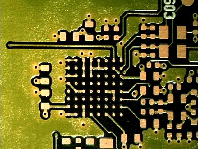
HDI PCBs: Unlocking High-Density Performance for Modern Electronics

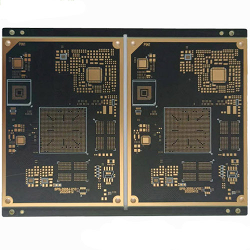
High-Density Interconnect (HDI) PCBs are a key technology for today’s compact and high-performance electronics. With fine lines, microvias, blind and buried vias, and multiple layers, HDI PCBs allow designers to fit complex circuits into small form factors, supporting applications from mobile devices to 5G infrastructure, automotive electronics, aerospace systems, and industrial IoT devices. Advanced Design...

Microvia PCB: The Ultimate Solution for HDI and High-Speed PCB Designs

In today’s rapidly evolving electronics market, devices are becoming smaller, faster, and more complex. To meet these demands, Microvia PCBs have become a critical solution in HDI PCB and high-speed PCB design. Microvias are extremely small vias that create precise interlayer connections, allowing for high-density routing, improved signal integrity, and reliable performance in modern electronic...

Engineering High Speed PCB for Signal Integrity, Low-Loss Routing, and Next-Generation Data Transmission

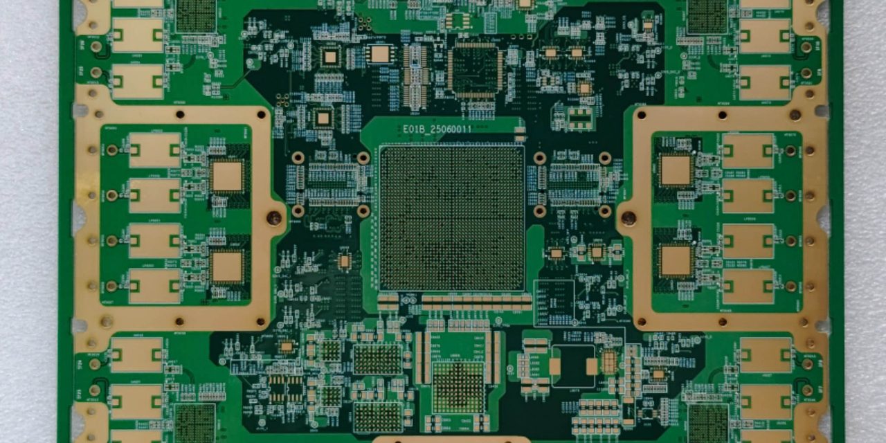
As digital systems move toward higher data rates, smaller form factors, and lower power consumption, the demand for High Speed PCB solutions continues to accelerate. From 10–112 Gbps SerDes links to DDR4/DDR5 memory buses and advanced communication modules, a High Speed PCB must deliver loss control, impedance stability, and electromagnetic reliability in increasingly complex environments....

HDI PCB: The Core Technology Driving Miniaturization and High-Performance Electronics

HDI PCB: The Foundation of Modern Electronic Miniaturization In today’s electronics industry, devices are becoming smaller, faster, and more powerful. To achieve this balance, engineers increasingly rely on HDI PCBs (High-Density Interconnect Printed Circuit Boards)—a technology that allows for higher circuit density, improved signal integrity, and enhanced performance within compact form factors. At KKPCB, we...

Mobile Phone PCB Layout: Key Considerations and Wiring Best Practices

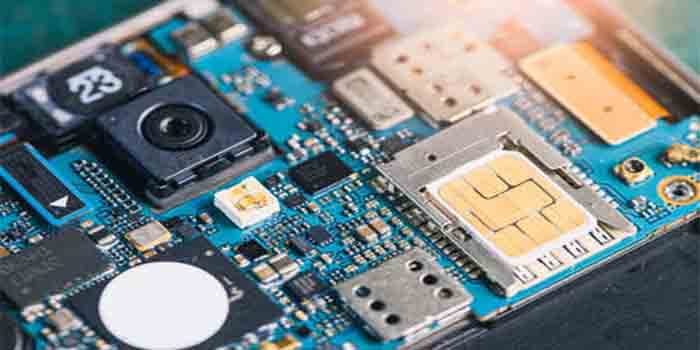
Engineering Context Modern smartphones integrate increasingly complex electronic functions into extremely compact form factors. A mobile phone PCB must support high-speed processors, 5G communication modules, RF front-end circuits, camera systems, power management units, sensors, wireless charging, and high-density memory devices while maintaining reliability and signal performance. Unlike traditional electronic boards, Mobile Phone PCB design requires...