Best Formats for 4-Layer PCB Stackups
A well-chosen 4-layer PCB stackup is essential for achieving excellent signal integrity, controlled impedance, effective power distribution, low EMI, and reliable manufacturing — especially in high-speed digital, mixed-signal, RF, automotive, and industrial designs. Compared to 2-layer boards, a properly configured 4-layer stackup provides dedicated reference planes, shorter return paths, higher routing density, and better noise isolation, making it the go-to choice for most modern electronics.
At KKPCB, we support a wide range of 4-layer PCB stackups tailored to customer needs, from standard FR-4 to high-frequency materials like Rogers, Megtron, and IS680. Our engineering team offers free DFM reviews to optimize your stackup for impedance control (±5% or better), minimal warpage, and cost-effective production.
Most Common and Recommended 4-Layer PCB Stackup Configurations
Here are the best-performing formats, ranked by popularity and suitability:
-
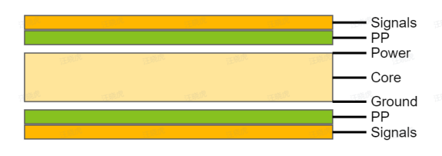
Signal – Ground – Power – Signal (SGPS) — The Industry Standard
- Layer 1: Signal (components + high-speed routing)
- Layer 2: Solid Ground Plane (GND)
- Layer 3: Power Plane (VCC or split planes)
- Layer 4: Signal (secondary routing)
Benefits:
- High-speed signals on Layer 1 reference a continuous ground plane for excellent return paths and low crosstalk.
- Tight coupling between GND and Power planes supports efficient decoupling.
- Predictable microstrip impedance on outer layers.
- Best overall balance for most digital, microcontroller, and FPGA designs operating above 50 MHz.
Best for: General high-speed digital, mixed-signal boards, consumer electronics, and industrial control.
-
Signal – Power – Ground – Signal (SPGS) — Alternative for Power-First Designs
- Layer 1: Signal
- Layer 2: Power Plane
- Layer 3: Ground Plane
- Layer 4: Signal
Benefits: Useful when power integrity is prioritized or when more signals need proximity to power. Considerations: Ground reference for Layer 1 signals is farther; requires careful decoupling.
-
Signal/Power – Ground – Ground – Signal/Power (SIG+PWR / GND / GND / SIG+PWR) — Superior for High-Speed & EMI
- Outer layers combine signals with routed power pours.
- Two solid internal ground planes provide excellent shielding and reference for signals on both sides.
Benefits:
- Outstanding EMI reduction and crosstalk suppression.
- Ideal for routing high-speed signals on both top and bottom layers.
- Strong return paths and low-inductance grounding.
Best for: High-speed digital (DDR, PCIe, SerDes), RF/microwave, automotive, and noise-sensitive applications.
-
Ground – Signal – Signal – Ground (GND / SIG / SIG / GND) — Shielded Cavity Style
- Outer layers are solid ground planes for maximum external EMI shielding.
- Inner layers handle all signal routing (including high-speed).
Benefits: Superior protection against external noise; excellent for sensitive analog or RF circuits. Trade-off: Slightly reduced outer-layer routing density.
Key Factors When Choosing the Best 4-Layer Stackup
- Signal Integrity & Impedance Control: Prefer configurations with a solid ground plane adjacent to critical signal layers (microstrip or stripline). Target 50 Ω single-ended or 100 Ω differential impedance.
- Power Integrity: Close GND-Power coupling reduces PDN impedance; use multiple decoupling capacitors.
- EMI/EMC Performance: Two ground planes or outer GND layers significantly improve shielding.
- Symmetry: Balanced copper distribution and dielectric thicknesses minimize warpage during reflow and thermal cycling — critical for automotive and industrial PCBs.
- Board Thickness: Common total thicknesses include 0.8 mm, 1.0 mm, 1.2 mm, 1.6 mm. Thinner boards suit compact devices; thicker for mechanical strength.
- Material Selection: FR-4 for cost-sensitive designs; high-Tg, low-loss (Megtron 6, IS680, Rogers RO3003) for RF, 77 GHz radar, or high-speed applications.
- Copper Weight: 1 oz standard; 2 oz on power layers for higher current.
Pro Tip: Always perform impedance modeling during DFM. KKPCB can adjust prepreg and core thicknesses to hit your exact impedance targets.
KKPCB’s Capabilities for 4-Layer PCB Stackups
- Flexible Stackup Options: Standard and custom configurations with tight tolerances on dielectric thickness (±5 µm) and registration.
- Advanced Materials: Support for high-frequency laminates, halogen-free, and automotive-grade substrates.
- Impedance Control: Precision etching and testing for consistent 50/100 Ω lines.
- One-Stop Service: From stackup optimization and Gerber review to full PCBA, functional testing, and mass production.
- Quality Assurance: IPC-6012 Class 2/3, IATF 16949, AOI, X-ray, and electrical testing for zero-defect delivery.
- Rapid Turnaround: Prototypes in 3–5 days; seamless scaling to volume.
Whether your project involves high-speed digital interfaces, RF antenna boards, ADAS radar, thermostat controls, or industrial IoT, the right 4-layer PCB stackup dramatically improves performance and reliability while controlling costs.
Ready to Optimize Your 4-Layer PCB Design?
Share your schematic, target impedance, frequency requirements, or board thickness with the KKPCB team. We provide:
- Free DFM analysis with recommended stackup formats
- Detailed layer drawings and impedance calculations
- Material recommendations and competitive quotes
- Expert guidance to minimize EMI, warpage, and manufacturing risks
Contact KKPCB today and let our engineers help you select the best 4-layer PCB stackup for superior signal integrity and first-pass success.
