
HomeTag

cavity PCB - KKPCB

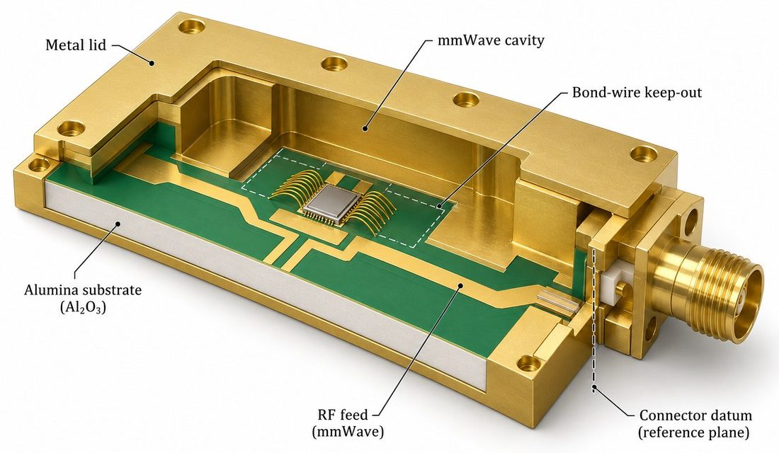
Alumina PCB for mmWave Packaging: Cavity, Ground, and Connector Datum Control

In a compact mmWave package, the Alumina PCB is often both circuit carrier and mechanical reference. A cavity, lid, bond window, connector, or waveguide transition can define the electromagnetic boundary more strongly than a long trace. The project risk is a datum mismatch: the electrical drawing references the board edge while the housing references the...
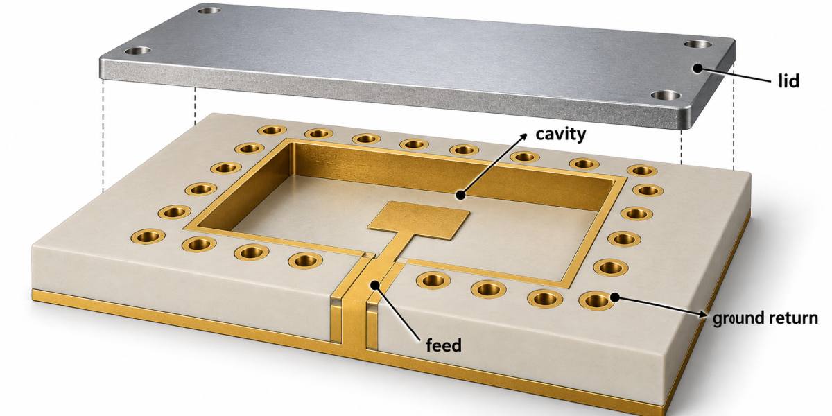
Ceramic PCB Antenna Cavities at mmWave: Controlling Geometry Before the First Build

At mmWave frequencies, the cavity, copper edge, connector launch, and antenna clearance become part of the circuit. A Ceramic PCB is often selected for its dimensional stability and integration potential, yet a cavity that is only slightly too deep or a ground fence that is interrupted by a tooling keep-out can move the resonance enough...