HomeCategory

Advanced Engineering Technologies for PCB & PCBA Solutions - KKPCB

PTFE PCB Glass-Weave and Phase Skew: A Routing Review for Wideband Links

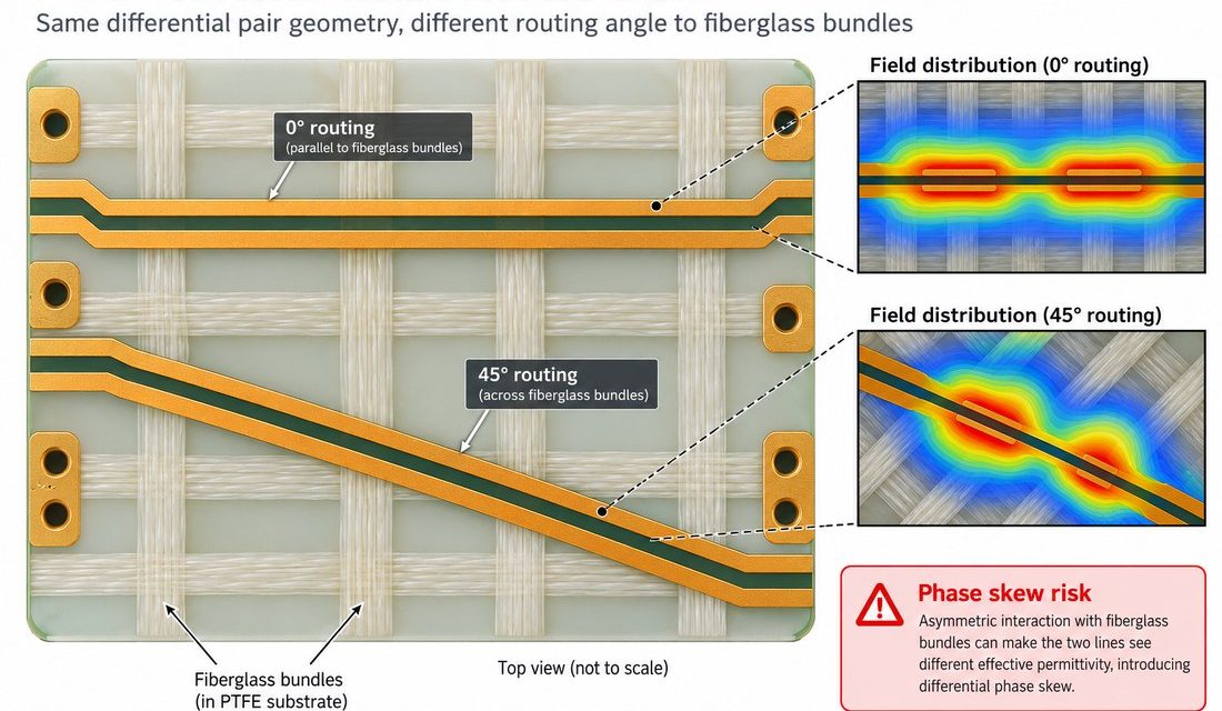
A wideband RF link can show unexplained phase imbalance even when both traces meet the same nominal impedance. On a PTFE PCB, the local resin-to-glass distribution, trace angle, reference-plane spacing, and connector launch can create different effective propagation paths. The project pain is usually discovered after the schematic is stable, when the pair is already...
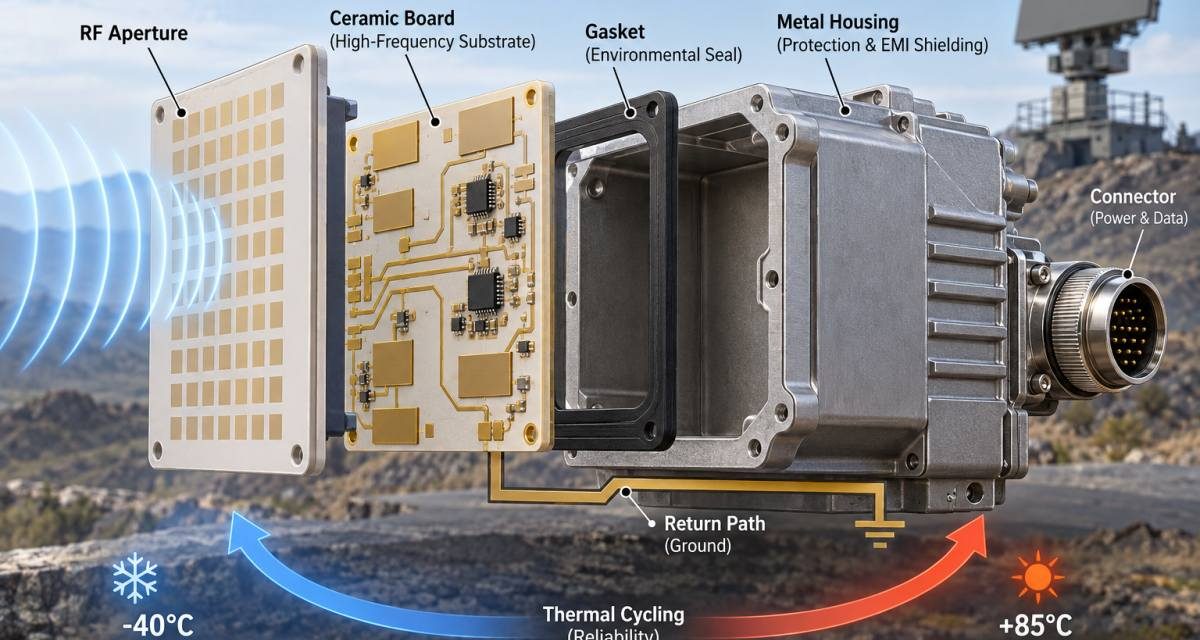
Ceramic PCB CTE and Moisture Decisions for Outdoor Radar and Sensor Modules

Outdoor radar and sensor hardware sees temperature swings, condensation risk, vibration, and repeated enclosure loads. A Ceramic PCB can reduce some dimensional and moisture-related uncertainty, but it does not remove the need to coordinate the ceramic, copper, seal, connector, and metal housing. The project pain appears when a material is chosen for a nominal dielectric...

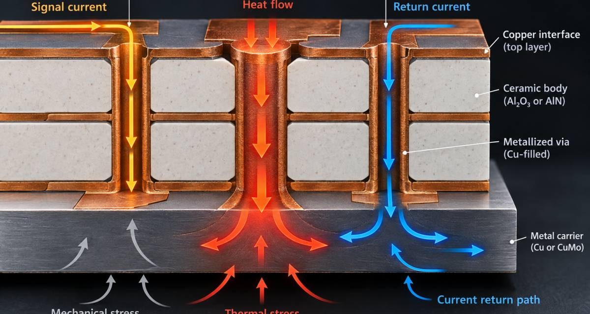
Ceramic PCB Metallization and Via Reliability: A Practical Review for RF Power Boards

A ceramic substrate can be electrically stable and thermally efficient while the interconnect still becomes the weak point. Metallization adhesion, plated or filled vias, copper thickness, and the transition to a connector or carrier all experience different mechanical strain. For a Ceramic PCB used in a power or microwave module, the correct question is not...

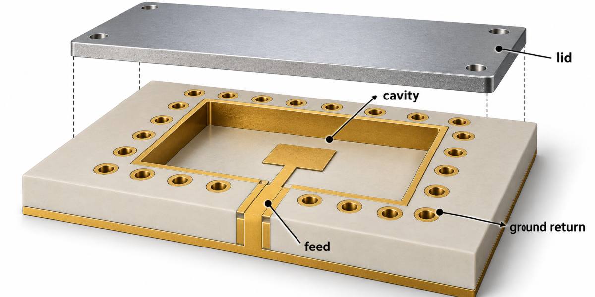
Ceramic PCB Antenna Cavities at mmWave: Controlling Geometry Before the First Build

At mmWave frequencies, the cavity, copper edge, connector launch, and antenna clearance become part of the circuit. A Ceramic PCB is often selected for its dimensional stability and integration potential, yet a cavity that is only slightly too deep or a ground fence that is interrupted by a tooling keep-out can move the resonance enough...

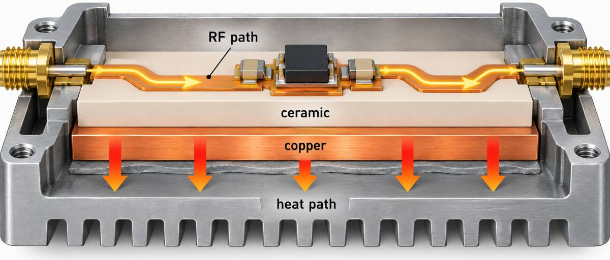
Ceramic PCB Thermal Interfaces for High-Power RF Modules: A Release Review

A high-power RF module can meet its electrical target and still fail in the field because the heat path was never released as a complete system. A Ceramic PCB changes the design conversation: the ceramic substrate, copper pattern, attach method, via or metallized interface, and the enclosure all share the same thermal boundary. The project...

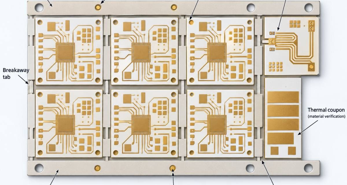
Ceramic PCB DFM and Procurement Release: Avoiding First-Build Surprises

Ceramic PCB programs often move from concept to purchase order faster than the manufacturing package matures. The layout may be complete, but the supplier still lacks a defined panel, edge condition, metallization note, inspection plan, or approved substitute rule. That gap creates schedule risk because a ceramic panel is not interchangeable with a conventional laminate...

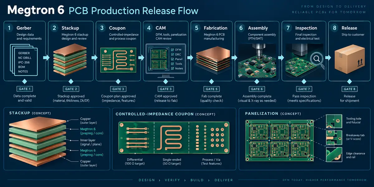
Megtron 6 PCB DFM Release: The Production Checks That Protect High-Speed Yield

The released Megtron 6 PCB construction is the reference for the DFM package. Any supplier change to a Megtron 6 PCB must carry the same stackup and coupon revision, so procurement can compare capacity without changing electrical intent. Megtron 6 PCB DFM release work is where a high-speed design becomes a repeatable production definition. A...

Megtron 6 PCB Assembly: A Reflow and Connector-Launch Plan for High-Speed Modules

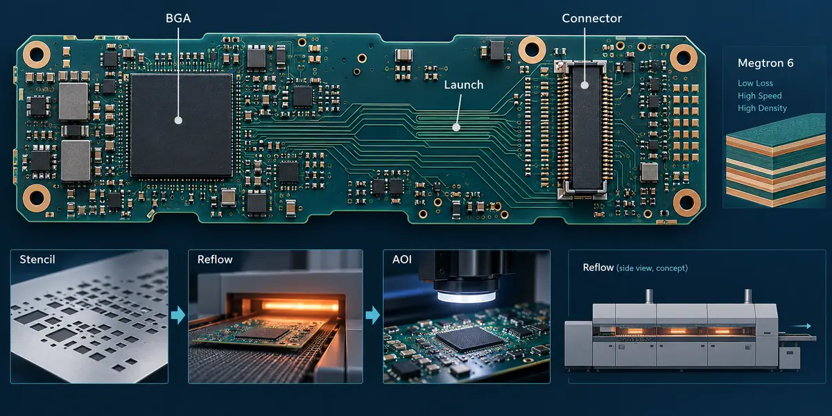
The Megtron 6 PCB connector launch remains the shared datum for SI and assembly inspection. The production Megtron 6 PCB callout should travel with the reflow and inspection package. A connector change on a Megtron 6 PCB is an electrical and assembly change, not only a mechanical edit. For the release team, a Megtron 6...

Megtron 6 PCB Thermal Cycling: Keeping Dense Multilayer Registration Predictable

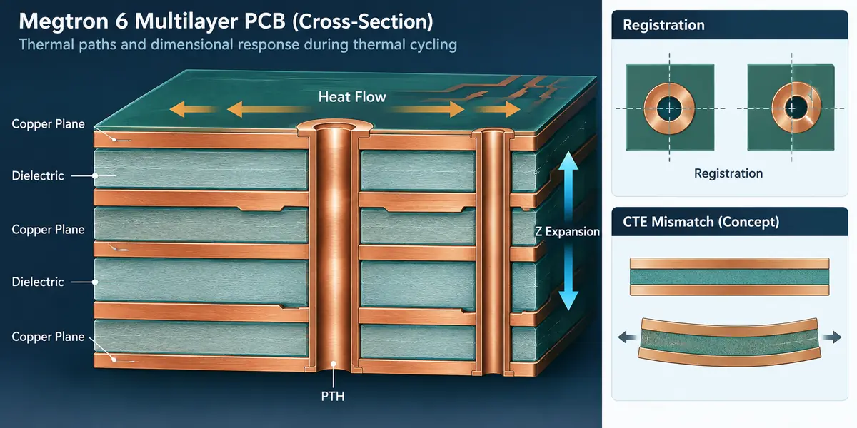
The controlled Megtron 6 PCB datum should be reviewed before thermal cycling begins. For a dense compute Megtron 6 PCB, copper balance and registration targets belong in the same release package. A second Megtron 6 PCB construction should never be approved without a revised coupon plan. Megtron 6 PCB thermal reliability is a registration problem...

Megtron 6 PCB for 112G Backplanes: Managing Skew, Vias, and Reference-Plane Continuity

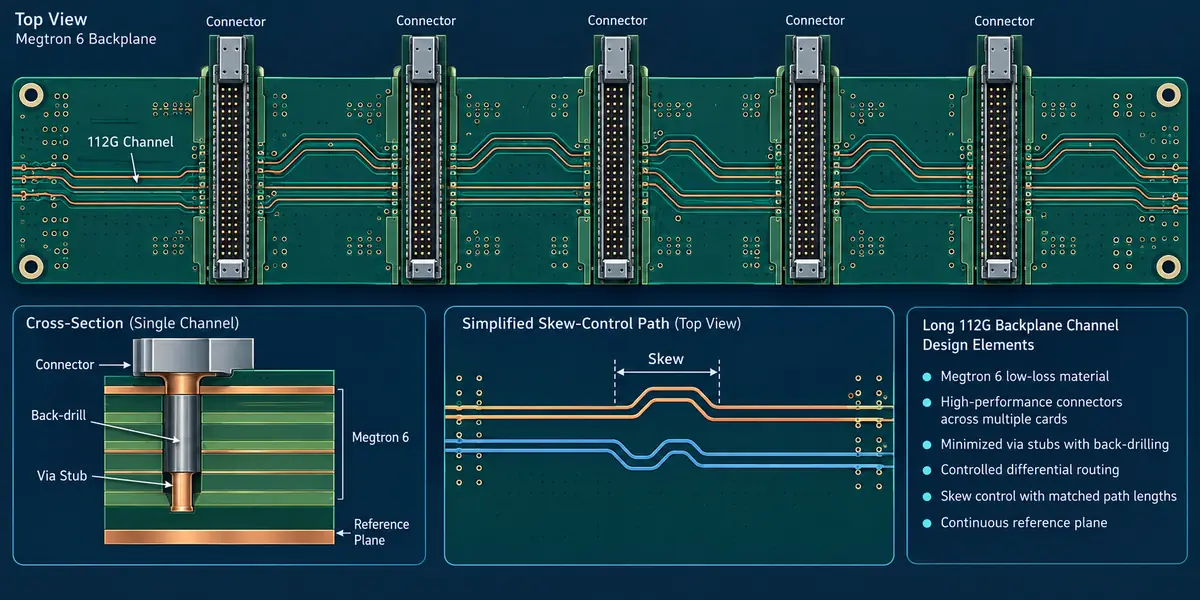
Table of Contents Channel construction Skew and weave control Via and plane continuity Coupon and release checks The released Megtron 6 PCB stackup must keep the 112G lane assumptions visible to design and fabrication. At this data rate, a small skew shift, a poorly referenced via field, or a connector launch that changes between panels...