
A wideband RF link can show unexplained phase imbalance even when both traces meet the same nominal impedance. On a PTFE PCB, the local resin-to-glass distribution, trace angle, reference-plane spacing, and connector launch can create different effective propagation paths. The project pain is usually discovered after the schematic is stable, when the pair is already routed and the only remaining change is an expensive board spin.
Treat the dielectric map as a routing constraint
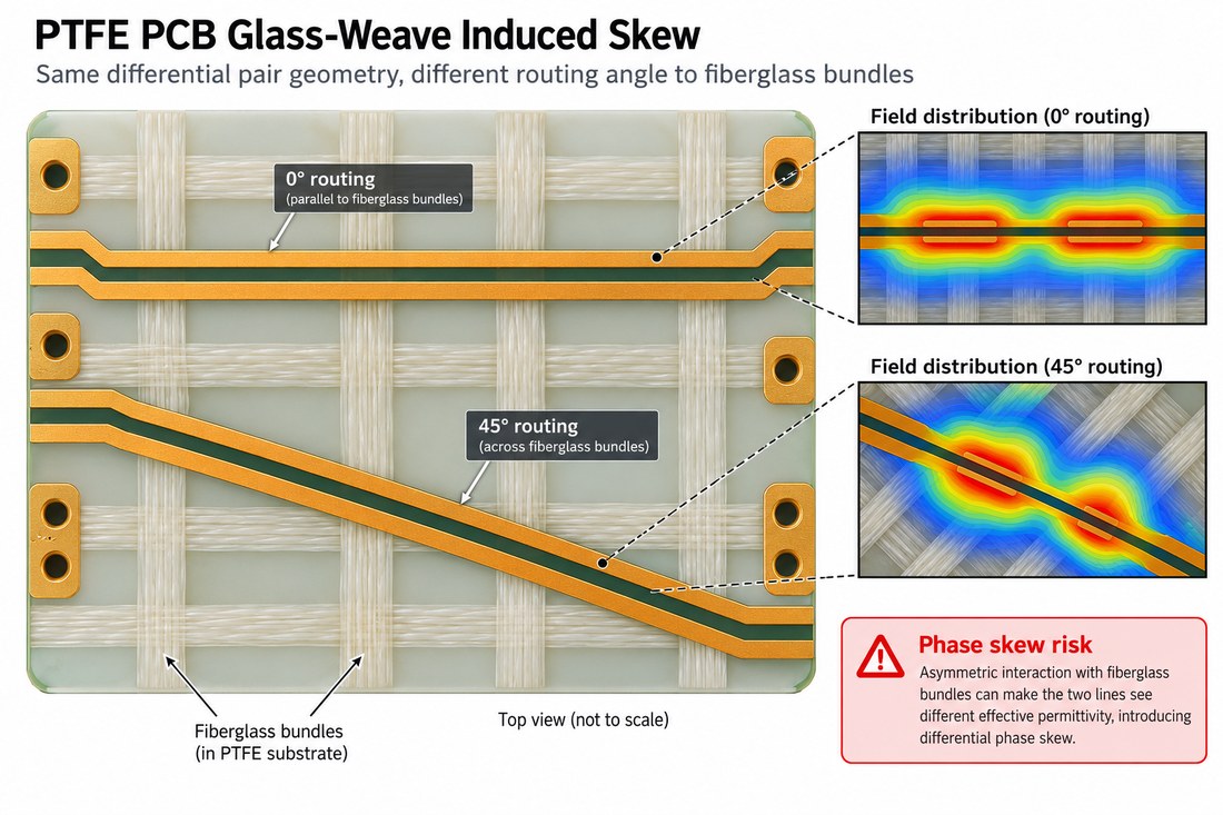
Start by identifying which line pairs are phase-sensitive and which are only amplitude matched. A PTFE PCB with woven reinforcement or a mixed construction should not be treated as a uniform dielectric slab at every coordinate. Route critical pairs with a consistent relationship to the weave and keep the pair away from abrupt resin-rich corners or cutouts.
Ask the material supplier for the design Dk method and construction notes, then use a field-solver model that matches the finished stack. The RF PCB design review should state the phase target, reference frequency range, and the assumed copper and surface finish. If the board house cannot guarantee a weave orientation, design margin into the phase budget.
For differential or I/Q links, keep the pair geometry symmetric through bends, pads, and layer changes. A return-path discontinuity can look like a material problem because it changes the local phase and amplitude together.
Use coupons that answer the phase question
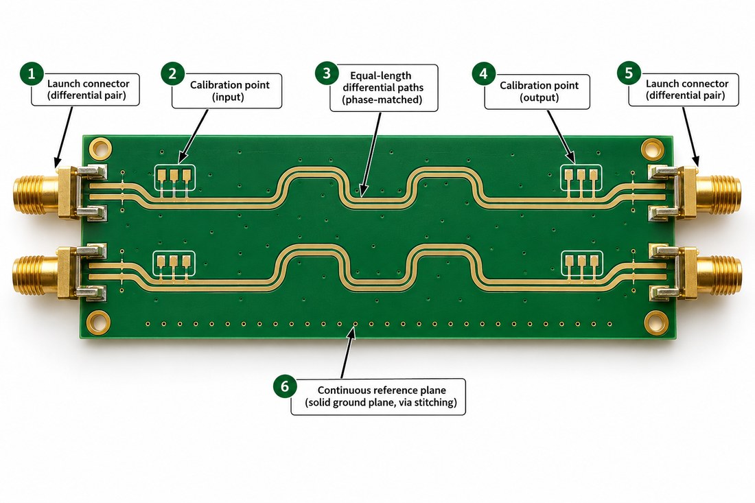
A generic impedance coupon can prove width and spacing but may not represent the phase-sensitive pair. The PTFE PCB coupon should preserve the line orientation, reference-plane spacing, copper treatment, and any via or connector transition that matters to the product.
The controlled impedance validation plan can compare delay or phase between two matched structures, but define the calibration, fixture, and sample identity before using a result in a release decision. A design target or engineering range must remain separate from a measured acceptance value.
Keep the pair away from panel rails and copper thieving changes if they alter the local stack. A panel drawing that shifts the pair relative to the weave or plating pattern may change the correlation even when the inner-layer artwork is unchanged.
Close the ECO loop
When a trace moves, update the phase budget and the coupon plan at the same time. The thermal management project record should show whether the move changes layer, angle, copper density, or connector launch. “Same length” is not enough if the electromagnetic environment changed.
If the material construction changes, re-run the pair review rather than copying the old delay number. PTFE systems with different reinforcement, filler, or copper treatment can have different phase behavior even when the nominal dielectric constant appears close.
Release a routing checklist with pair class, weave strategy, symmetry, return path, coupon, and ECO owner. This gives both the layout engineer and the project manager a measurable handoff.
PTFE PCB phase balance is controlled by routing and construction together. Give the critical pair a defined dielectric environment, a representative coupon, and a change-control trigger before the first prototype.
Implementation note for this glass weave and phase balance review: keep the engineering assumption visible at the point where it affects a drawing, a supplier quote, or an inspection record. Ask the design owner to identify the reference plane, interface datum, and acceptance method before the release is frozen. Ask manufacturing to return the proposed stack, panel, and process window rather than a generic capability statement. Ask assembly to identify the profile, cleaning, and support conditions that could move the RF or thermal result. This simple handoff prevents a typical material value from being mistaken for a guaranteed product result and gives the project team a clear action when an ECO changes the physical boundary.
Release note: keep the PTFE PCB phase target tied to the approved weave orientation, pair geometry, and coupon so a layout ECO can be correlated before release.
For a PTFE PCB phase review, compare the PTFE PCB pair against the same released construction, orientation, and return-path assumptions before accepting a phase result.
Sources: Panasonic MEGTRON technical material guidance; Rogers and Taconic high-frequency material data sheets where relevant; CeramTec ceramic substrate data; Analog Devices RF and mixed-signal layout guidance. Numerical values are treated as typical supplier values or engineering targets unless the released drawing defines a measured acceptance value.
Release note: confirm the PTFE PCB construction before the next ECO.
Release note: confirm the PTFE PCB construction before the next ECO.
Release note: confirm the PCB manufacturing evidence before approval.
Release note: confirm the PCB assembly evidence before approval.
