HomeTag

Controlled Impedance - KKPCB

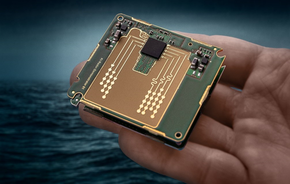
RO3003 PCB: Low Loss RF Material for Microwave Applications

As RF and microwave systems continue to expand in industries such as 5G communications, automotive radar, satellite equipment, and wireless networking, the choice of PCB material becomes critical. At high frequencies, signal integrity and loss performance can no longer rely on standard FR4. RO3003 PCB is a popular solution for high-frequency applications because it provides...
Engineering High Speed PCB for Signal Integrity, Low-Loss Routing, and Next-Generation Data Transmission

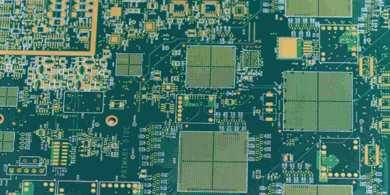
As digital systems move toward higher data rates, smaller form factors, and lower power consumption, the demand for High Speed PCB solutions continues to accelerate. From 10–112 Gbps SerDes links to DDR4/DDR5 memory buses and advanced communication modules, a High Speed PCB must deliver loss control, impedance stability, and electromagnetic reliability in increasingly complex environments....

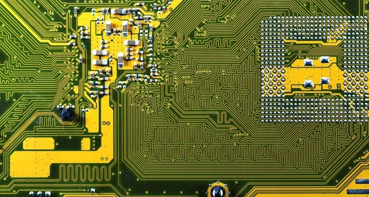
Enhance Signal Integrity and High-Speed Stability with Impedance Controlled PCB Platforms for 5G Communication Systems

5G communication systems rely on stringent impedance accuracy, low insertion loss, and predictable phase stability to maintain signal integrity across multi-gigabit transmission channels. At mmWave and sub-6 GHz bands, even slight deviations in controlled impedance routing can introduce reflection, jitter accumulation, and eye-diagram degradation.Impedance Controlled PCBs engineered for 5G must balance dielectric uniformity, copper surface...

Improving Dielectric Consistency and RF Efficiency of Megtron 6 PCBs for Industrial IoT and Wireless Sensor Networks

In the fast-growing world of Industrial IoT (IIoT) and Wireless Sensor Networks (WSN), reliable wireless communication is essential for real-time monitoring, predictive maintenance, and smart factory operations. Megtron 6, Panasonic’s high-performance low-loss PCB material, is widely chosen for these applications because of its excellent dielectric properties: stable Dk (dielectric constant) around 3.2–3.6 and ultra-low Df...

Exploring Teflon PCBs: The Ultimate Guide to High-Frequency and RF Applications

Introduction With the rapid advancement of modern technology, high-frequency electronic systems such as RF, microwave, and radar equipment are increasingly prevalent. At the core of these systems lies the Printed Circuit Board (PCB) — the foundation upon which signal integrity and overall device performance depend. Among the materials used for PCB fabrication, Teflon (PTFE) stands...

Next-Generation 5G PCB Design: Materials, Layout & Engineering Challenges

Introduction 5G is not just an upgrade from 4G—it represents a technological leap forward in global connectivity. With ultra-high speed, wide bandwidth, and expanded frequency ranges such as sub-6 GHz and millimeter wave (mmWave), 5G transforms how devices communicate.At the core of this revolution lies one critical component — the Printed Circuit Board (PCB). A...

About PCB Layer Stackup

A PCB Layer Stackup refers to the arrangement of conductive copper layers and insulating dielectric materials that make up a multilayer PCB. In the era of high-speed digital electronics and 5G, the stackup is no longer just a mechanical carrier; it is a critical tool for managing signal integrity, power distribution, and electromagnetic compatibility (EMC). A well-engineered stackup from KKPCB ensures...

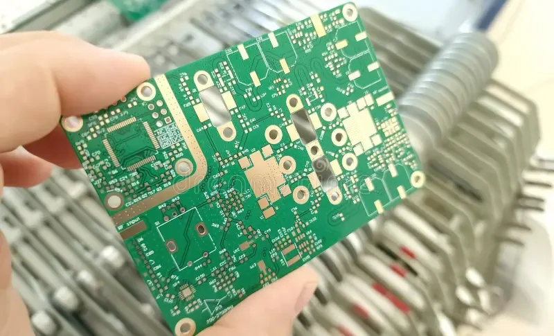
How to avoid radio frequency and microwave PCB design issues

With the rapid development of wireless communication, radar systems, satellite communication, automotive electronics, and high-frequency industrial applications, RF (Radio Frequency) and microwave PCB technology has become increasingly important. Unlike conventional low-frequency PCB designs, RF and microwave circuits operate at higher frequencies where even small variations in PCB structure can significantly affect electrical performance. Common design...

Best Formats for 4-Layer PCB Stackups

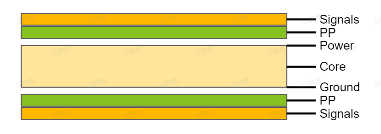
Best Formats for 4-Layer PCB Stackups A well-chosen 4-layer PCB stackup is essential for achieving excellent signal integrity, controlled impedance, effective power distribution, low EMI, and reliable manufacturing — especially in high-speed digital, mixed-signal, RF, automotive, and industrial designs. Compared to 2-layer boards, a properly configured 4-layer stackup provides dedicated reference planes, shorter return paths,...

Manufacturing Optimization Case: Mass Production Solution for 256-Channel Phased Array Antenna Feed Network PCBs

Engineering Context / Abstract Mass production of a 256-channel phased array antenna feed network PCB is fundamentally different from building a small RF prototype. Trace-width or dielectric-thickness variation is repeated across hundreds of signal paths and becomes a system-level error in beam direction, gain distribution, sidelobe control, and calibration stability. This manufacturing optimization case involved...