
With the rapid development of wireless communication, radar systems, satellite communication, automotive electronics, and high-frequency industrial applications, RF (Radio Frequency) and microwave PCB technology has become increasingly important.
Unlike conventional low-frequency PCB designs, RF and microwave circuits operate at higher frequencies where even small variations in PCB structure can significantly affect electrical performance.
Common design issues include:
- Signal loss
- Impedance mismatch
- Crosstalk
- Phase variation
- Electromagnetic interference (EMI)
- Reduced transmission efficiency
To achieve stable RF performance, engineers must consider the entire PCB development process, including material selection, stack-up design, layout optimization, manufacturing capability, and testing requirements.
1. Understanding the Challenges of RF and Microwave PCB Design
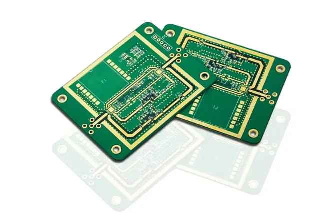
1.1 High-Frequency Signal Sensitivity
At microwave frequencies, signals are highly sensitive to physical changes in PCB structures.
Factors that can affect performance include:
- Trace width variation
- Dielectric thickness changes
- Copper surface roughness
- Material tolerance
- Connector transitions
Small design deviations can cause measurable changes in:
- Insertion loss
- Return loss
- Signal phase
- Antenna performance
1.2 Complex Electromagnetic Behavior
RF signals behave differently from low-frequency signals.
At high frequencies:
- Current distribution becomes non-uniform
- Transmission lines become critical structures
- Parasitic effects become more significant
Therefore, RF PCB traces should be treated as controlled transmission lines rather than simple connections.
2. Select the Right PCB Material
2.1 Avoid Using Unsuitable Substrate Materials
Material selection is one of the most important factors in RF PCB design.
Traditional FR-4 materials may have limitations in high-frequency applications due to:
- Higher dielectric loss
- Greater dielectric variation
- Higher signal attenuation
For RF and microwave circuits, engineers often select specialized materials such as:
- Rogers high-frequency laminates
- PTFE-based materials
- Low-loss microwave substrates
2.2 Consider Key Material Parameters
Important material characteristics include:
Dielectric Constant (Dk)
The dielectric constant affects:
- Signal propagation speed
- Impedance calculation
- Phase stability
Stable Dk values are important for precise RF performance.
Loss Tangent (Df)
A lower loss tangent helps reduce:
- Transmission loss
- Energy dissipation
This is critical for:
- Microwave circuits
- Long-distance RF transmission
Thermal Stability
RF materials should maintain stable electrical properties under temperature changes.
Important considerations include:
- Temperature coefficient of Dk
- Thermal expansion characteristics
3. Optimize RF PCB Stack-Up Design
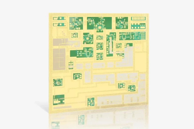
3.1 Maintain Proper Layer Arrangement
A well-designed stack-up provides:
- Stable impedance
- Continuous reference planes
- Better electromagnetic performance
Engineers should carefully define:
- Signal layers
- Ground planes
- Power layers
- Dielectric thickness
3.2 Avoid Poor Reference Plane Design
RF signals require stable return current paths.
Problems may occur when signals cross:
- Ground plane gaps
- Split planes
- Layer transitions without proper grounding
These conditions may cause:
- Increased radiation
- Impedance discontinuity
- Signal degradation
4. Control Impedance During RF PCB Design
4.1 Design Controlled Impedance Transmission Lines
RF traces should be designed according to target impedance requirements.
Common impedance values include:
- 50Ω single-ended impedance
- 100Ω differential impedance
Parameters affecting impedance include:
- Trace width
- Copper thickness
- Dielectric thickness
- Material properties
4.2 Avoid Sudden Impedance Changes
Common causes of impedance discontinuity include:
- Sharp corners
- Sudden width changes
- Improper vias
- Connector transitions
Recommended practices:
- Use smooth routing transitions
- Optimize via structures
- Maintain consistent geometry
5. Improve RF PCB Layout and Routing
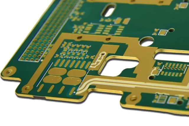
5.1 Keep RF Signal Paths Short
Long RF traces increase:
- Signal loss
- Phase variation
- Radiation risk
Critical RF paths should be:
- Short
- Direct
- Carefully controlled
5.2 Avoid Sharp Corners
Sharp 90-degree bends may create:
- Impedance discontinuity
- Current concentration
Better solutions include:
- 45-degree routing
- Curved traces
5.3 Maintain Adequate Isolation
RF circuits are sensitive to interference.
Engineers should separate:
- RF circuits
- Digital circuits
- Switching power sections
Proper isolation helps reduce:
- Crosstalk
- EMI problems
6. Grounding and Shielding Considerations
6.1 Use Effective Grounding Structures
Good RF grounding practices include:
- Continuous ground planes
- Proper via stitching
- Short grounding paths
These help improve:
- Signal integrity
- EMI performance
6.2 Optimize Via Fence Design
Via fences are commonly used around RF transmission lines.
Benefits include:
- Reduced electromagnetic leakage
- Improved isolation
- Better RF containment
7. Pay Attention to RF Component Placement
7.1 Minimize Interconnection Distance
RF components should be placed according to signal flow.
Examples:
- Antenna → RF filter → Amplifier → Transceiver
Shorter connections reduce:
- Loss
- Unwanted coupling
7.2 Separate Sensitive RF Blocks
Sensitive circuits should be isolated from:
- High-speed digital circuits
- Power switching circuits
This reduces interference and improves system stability.
8. Manufacturing Considerations for RF and Microwave PCB
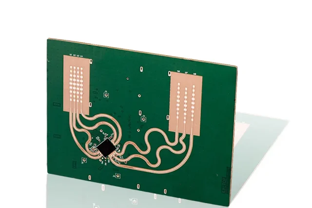
8.1 Maintain Manufacturing Tolerance
RF performance depends heavily on manufacturing accuracy.
Important controls include:
- Trace width tolerance
- Dielectric thickness tolerance
- Layer alignment
- Copper thickness consistency
8.2 Surface Finish Selection
Surface finish can influence high-frequency performance.
Considerations include:
- Surface roughness
- Conductor loss
- Assembly reliability
Suitable finishes should balance:
- Electrical performance
- Manufacturing requirements
8.3 Control Copper Surface Roughness
At high frequencies, signals tend to travel along conductor surfaces due to the skin effect.
Excessive copper roughness can increase:
- Insertion loss
- Signal attenuation
Low-roughness copper materials may be required for advanced RF designs.
9. RF PCB Testing and Validation
9.1 Impedance Testing
TDR testing helps verify:
- Actual impedance values
- Transmission line consistency
9.2 RF Performance Testing
Depending on application requirements, testing may include:
- Network analyzer measurement
- Insertion loss testing
- Return loss testing
- VSWR testing
9.3 Prototype Validation
Before mass production, prototype evaluation helps identify:
- Layout issues
- Material performance differences
- Manufacturing limitations
10. Common RF and Microwave PCB Design Mistakes
Incorrect Material Selection
Problem:
Using standard materials for high-frequency applications.
Result:
- Increased signal loss
- Poor phase stability
Poor Impedance Control
Problem:
Ignoring transmission line characteristics.
Result:
- Reflection
- Signal distortion
Improper Ground Design
Problem:
Broken return paths.
Result:
- EMI problems
- Reduced RF performance
Excessive Routing Length
Problem:
Long RF paths.
Result:
- Increased attenuation
- Phase variation
Conclusion
RF and microwave PCB design requires a comprehensive understanding of high-frequency signal behavior, material properties, electromagnetic effects, and manufacturing limitations.
Avoiding common design issues requires careful control of:
- PCB material selection
- Stack-up structure
- Impedance design
- RF layout
- Grounding strategy
- Manufacturing process
By applying proper RF engineering principles and working closely with PCB manufacturers during the design stage, engineers can improve signal integrity, reduce development risks, and achieve reliable high-frequency electronic products.

