HomeTag

high-speed PCB - KKPCB

Aerospace PCB Design for FPGA Flight Computers: Stackup, PDN, and Return-Path Tradeoffs

Table of Contents Why a flight-computer board needs an SI/PI-first layout study Build the stackup around the package escape and power loop Translate FPGA load steps into a PDN verification plan Protect high-speed returns through connectors and board boundaries Make the mechanical and manufacturing boundary explicit Use release evidence that survives a late component or...
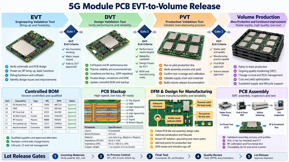
From EVT Evidence to Volume Release for a 5G Module PCB

5G module PCB production release begins when design evidence, supplier capability, and change control agree. The last ten percent of a board program is rarely a single design change. It is the point where a prototype stackup, a supplier process, a connector choice, and an enclosure must become one controlled release. For compact radio modules...

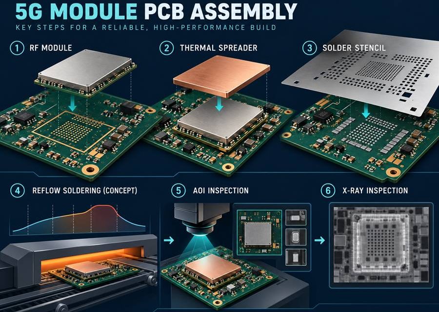
Keeping RF Performance Intact Through 5G Module PCB Assembly

5G module PCB assembly release begins by treating heat, solder, cleaning, and mechanical force as RF variables. An RF board can leave fabrication within drawing limits and still change during paste printing, reflow, shielding, cleaning, or mechanical assembly. That risk is amplified in compact radio modules used in private 5G radios, fixed-wireless units, and edge...

Designing Connector and Via Transitions for a 5G Module PCB Launch

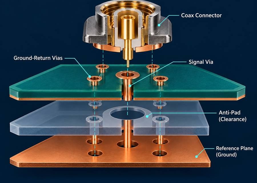
5G module PCB launch design begins with a complete three-dimensional signal and return path. The boundary between a board and a connector, coax, antenna, or shield is where a clean schematic becomes a three-dimensional electromagnetic problem. In compact radio modules used in private 5G radios, fixed-wireless units, and edge gateways, that boundary can set the...

Selecting a 5G Module PCB Stackup Without Hiding the Loss Budget

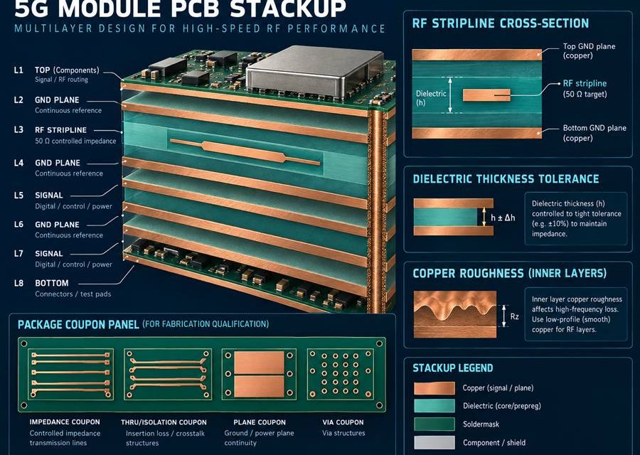
5G module PCB stackup release begins by making every electromagnetic and manufacturing assumption visible. Stackup discussions fail when the drawing lists layer names but not the electromagnetic and manufacturing assumptions behind them. In compact radio modules used in private 5G radios, fixed-wireless units, and edge gateways, the board must carry RF energy, power current, high-speed...

Megtron 7 PCB Copper Profile and Glass-Weave Control for Long Backplane Channels

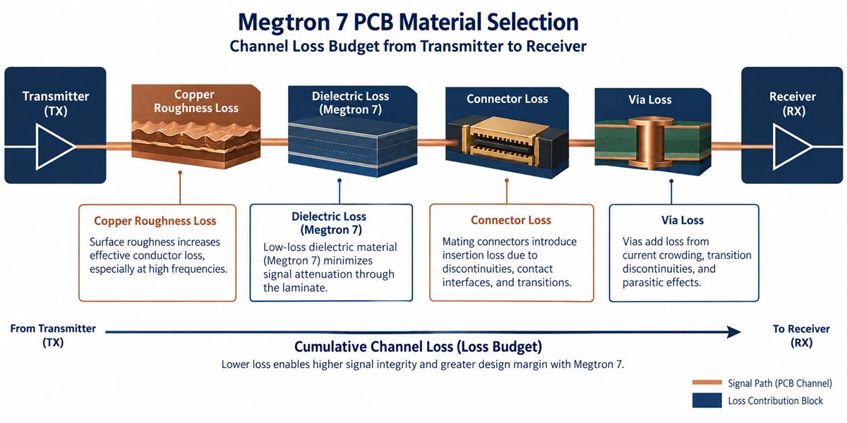
A long backplane channel can fail a design review even when the laminate choice looks correct on paper. The usual problem is not one dramatic defect; it is the accumulation of copper profile loss, dielectric loss, connector discontinuity, via loss, and local glass-weave skew. A useful Megtron 7 PCB project therefore starts with a channel...

Megtron 6 PCB Assembly: A Reflow and Connector-Launch Plan for High-Speed Modules

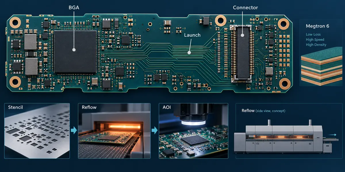
The Megtron 6 PCB connector launch remains the shared datum for SI and assembly inspection. The production Megtron 6 PCB callout should travel with the reflow and inspection package. A connector change on a Megtron 6 PCB is an electrical and assembly change, not only a mechanical edit. For the release team, a Megtron 6...

Megtron 6 PCB Thermal Cycling: Keeping Dense Multilayer Registration Predictable

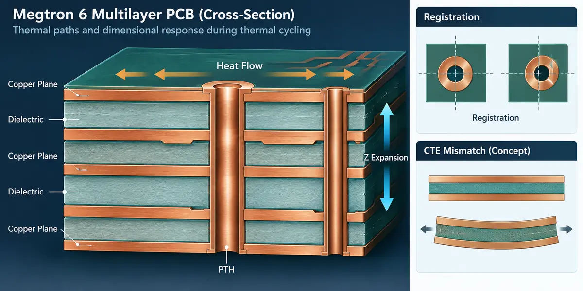
The controlled Megtron 6 PCB datum should be reviewed before thermal cycling begins. For a dense compute Megtron 6 PCB, copper balance and registration targets belong in the same release package. A second Megtron 6 PCB construction should never be approved without a revised coupon plan. Megtron 6 PCB thermal reliability is a registration problem...

Megtron 6 PCB for 112G Backplanes: Managing Skew, Vias, and Reference-Plane Continuity

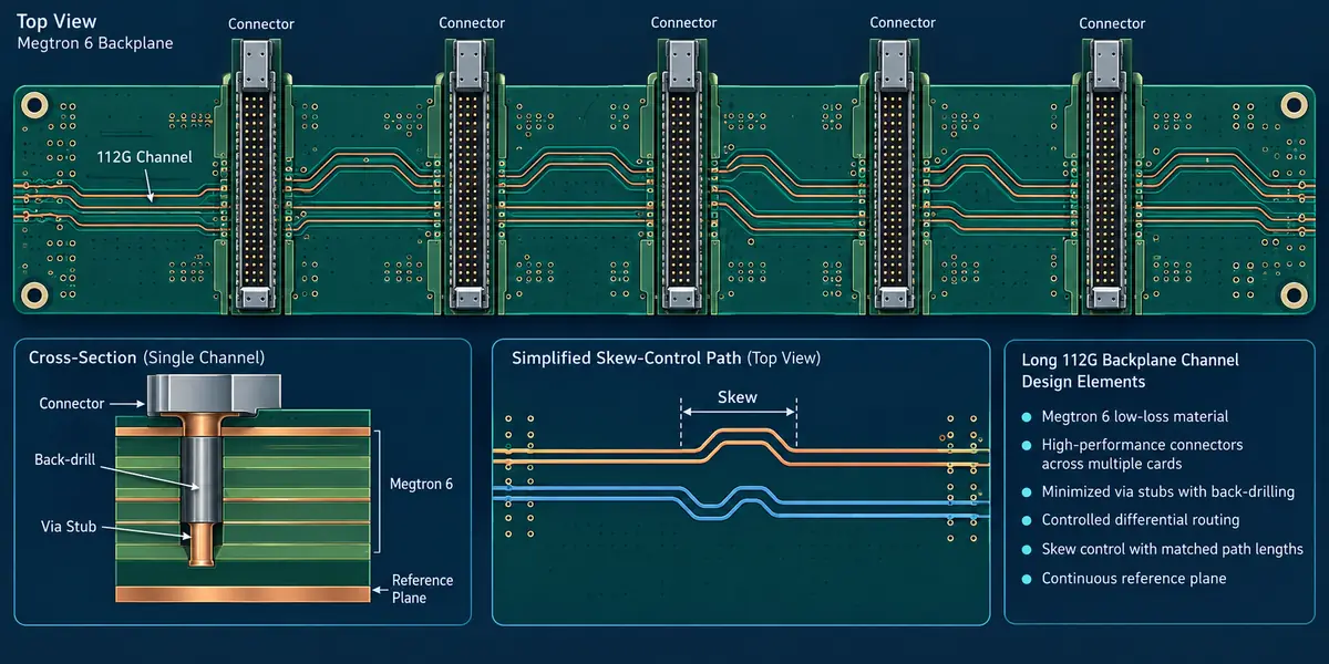
Table of Contents Channel construction Skew and weave control Via and plane continuity Coupon and release checks The released Megtron 6 PCB stackup must keep the 112G lane assumptions visible to design and fabrication. At this data rate, a small skew shift, a poorly referenced via field, or a connector launch that changes between panels...

Megtron 6 PCB Material Selection: Turning Loss Budgets into a Manufacturable Stackup

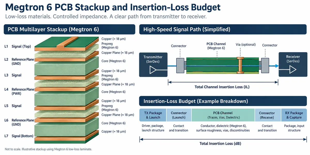
Megtron 6 PCB projects often fail late for a simple reason: the electrical loss budget was written before the stackup, copper profile, and connector geometry were frozen. A material family can support demanding high-speed channels, but the released board still depends on resin content, finished dielectric thickness, reference-plane continuity, copper roughness, and fabrication capability. This...