HomeCategory

PCB Design Services | Professional PCB Layout & Design - KKPCB

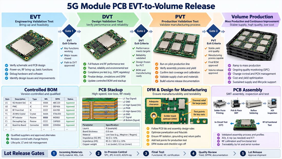
From EVT Evidence to Volume Release for a 5G Module PCB

5G module PCB production release begins when design evidence, supplier capability, and change control agree. The last ten percent of a board program is rarely a single design change. It is the point where a prototype stackup, a supplier process, a connector choice, and an enclosure must become one controlled release. For compact radio modules...
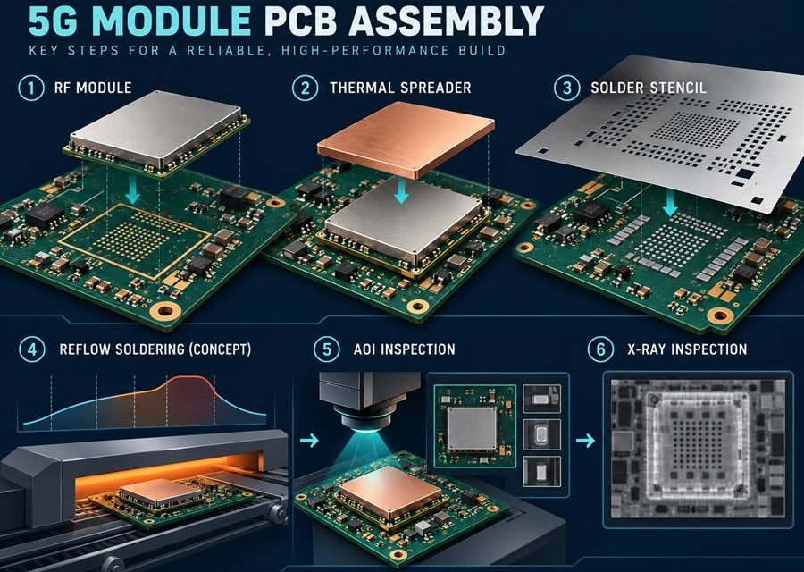
Keeping RF Performance Intact Through 5G Module PCB Assembly

5G module PCB assembly release begins by treating heat, solder, cleaning, and mechanical force as RF variables. An RF board can leave fabrication within drawing limits and still change during paste printing, reflow, shielding, cleaning, or mechanical assembly. That risk is amplified in compact radio modules used in private 5G radios, fixed-wireless units, and edge...

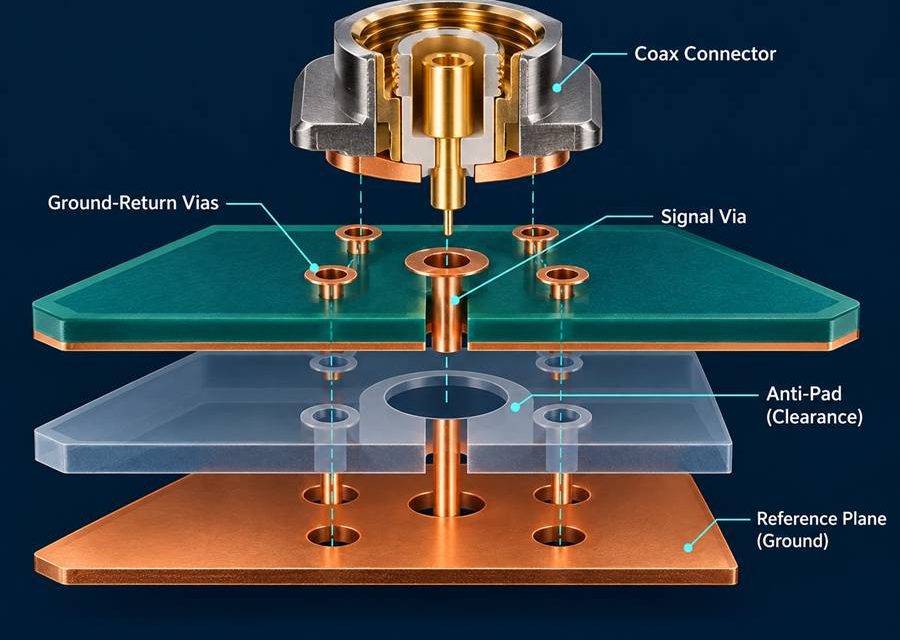
Designing Connector and Via Transitions for a 5G Module PCB Launch

5G module PCB launch design begins with a complete three-dimensional signal and return path. The boundary between a board and a connector, coax, antenna, or shield is where a clean schematic becomes a three-dimensional electromagnetic problem. In compact radio modules used in private 5G radios, fixed-wireless units, and edge gateways, that boundary can set the...

Selecting a 5G Module PCB Stackup Without Hiding the Loss Budget

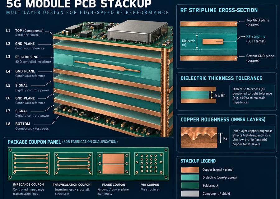
5G module PCB stackup release begins by making every electromagnetic and manufacturing assumption visible. Stackup discussions fail when the drawing lists layer names but not the electromagnetic and manufacturing assumptions behind them. In compact radio modules used in private 5G radios, fixed-wireless units, and edge gateways, the board must carry RF energy, power current, high-speed...

Aluminum Nitride PCB Inverter Modules: DFM, Panel Handling, and Production Release Controls

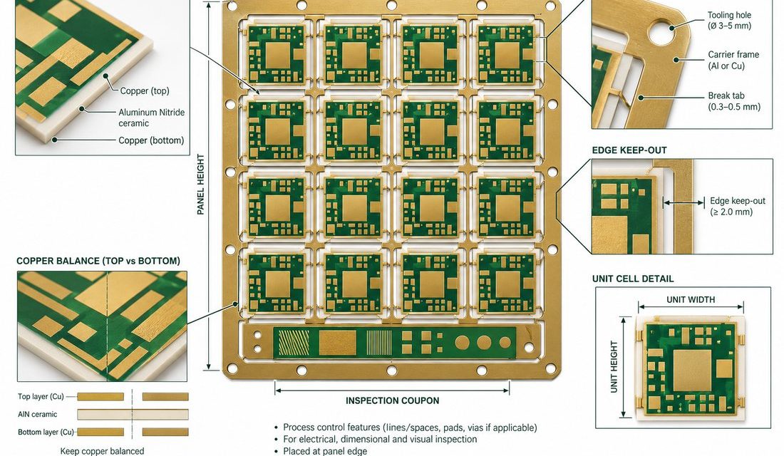
An Aluminum Nitride PCB inverter module release should connect panel handling, copper interfaces, and inspection evidence before production volume is authorized. Inverter modules expose the difference between a ceramic concept and a repeatable production process. Heavy copper, AlN substrate, switching devices, isolation clearances, carrier support, and inspection access all compete for the same panel area....

Aluminum Nitride PCB for mmWave Sensor Carriers: Geometry, Return Paths, and Thermal Margins

An Aluminum Nitride PCB sensor carrier must keep package geometry, RF return, and thermal margin visible in one controlled interface drawing. An mmWave sensor carrier must keep the feed geometry stable while moving heat away from the active device and preserving the enclosure datum. Aluminum nitride can support that combination, yet the first build can...

Aluminum Nitride PCB RF Power Layout: Separating Return Current from Heat Spreading

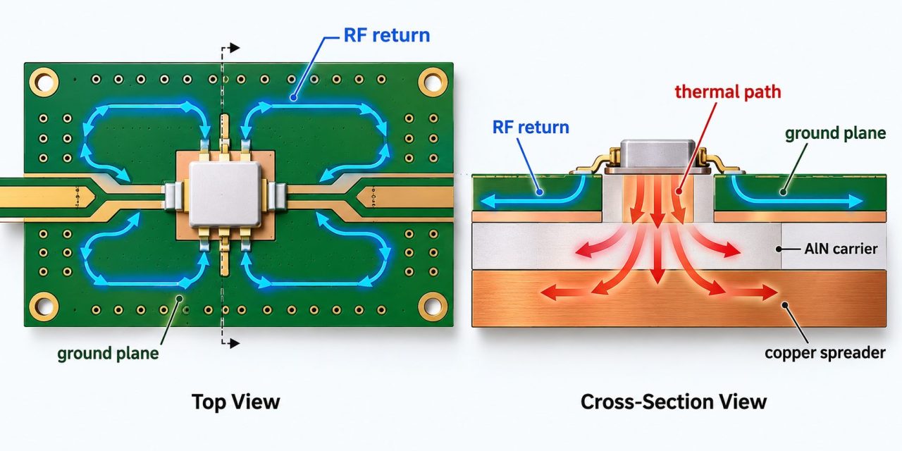
An Aluminum Nitride PCB power layout must release current return and heat through the same controlled interface before the module is approved. RF power boards built on aluminum nitride combine a low-loss electrical path with a high-conductivity thermal path, but the two paths do not always want the same copper geometry. A power island may...

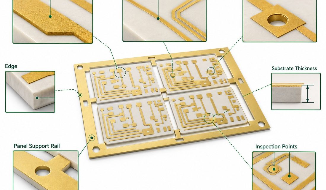
Alumina PCB DFM: Metallization, Panel Handling, and Inspection Before Volume Release

Volume release exposes the difference between a ceramic layout and a ceramic process. Screen, thick-film, thin-film, plated, brazed, and bonded features each have a different capability window. An Alumina PCB drawing that specifies only line widths and hole sizes can still leave the supplier guessing about paste, firing, edge handling, carrier support, and inspection. The...

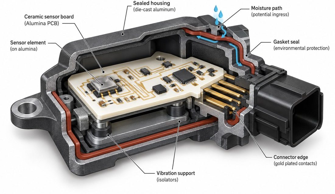
Alumina PCB for Automotive Sensors: Moisture, Vibration, and Connector Edge Decisions

Automotive sensor modules combine a ceramic substrate with a connector, housing, adhesive, shield, and sometimes a high-frequency antenna. The Alumina PCB is stable, but the assembled module still sees vibration, thermal cycling, condensation, and connector loads. The project pain is often a fracture or intermittent contact at an edge feature that was reviewed only as...

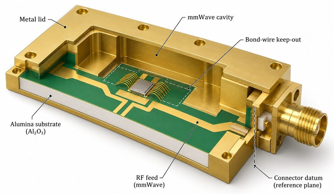
Alumina PCB for mmWave Packaging: Cavity, Ground, and Connector Datum Control

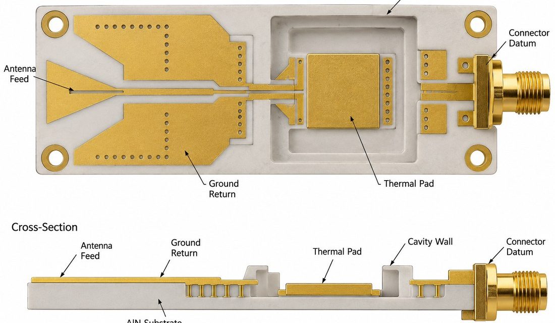
In a compact mmWave package, the Alumina PCB is often both circuit carrier and mechanical reference. A cavity, lid, bond window, connector, or waveguide transition can define the electromagnetic boundary more strongly than a long trace. The project risk is a datum mismatch: the electrical drawing references the board edge while the housing references the...