Blog

Explore the KKPCB Blog for the latest PCB manufacturing and assembly news, industry insights, expert tips, and technology trends, helping you stay informed and optimize your electronics projects.
Skin Effect in 5G PCB Manufacturing

Every 5G PCB project eventually arrives at the same question: how much does the skin effect really cost the design? The answer is rarely a single number, because the effect grows with frequency and depends on decisions taken across the stackup, the layout and the fabrication process. At high-frequency bands, a board that looks acceptable...

PCB Material Characterization: Test Methods for High-Frequency and mmWave PCB

Why PCB Material Characterization Matters at High Frequencies The electrical properties of a PCB material can be characterized using several different measurement techniques. Some methods directly evaluate the dielectric material using specialized fixtures, while others characterize the material through an actual circuit structure. This distinction becomes increasingly important as PCB operating frequencies move from conventional...

How to Choose Materials for Millimeter-Wave and Multilayer PCB Design

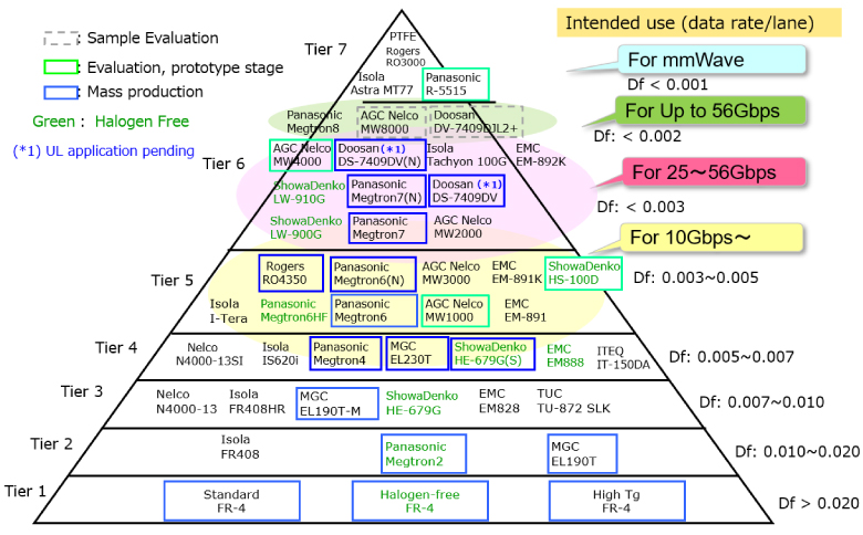
Why Material Selection Matters in Millimeter-Wave PCB Design Millimeter-wave technology was once considered too expensive or technically difficult for widespread commercial applications. Today, that has changed rapidly. The expansion of 5G New Radio (5G NR), 77 GHz automotive radar, ADAS, high-speed wireless communication, RF modules, and advanced sensing systems has made millimeter-wave PCB technology increasingly...