HomeCategory

PCB Manufacturing Services | High-Quality PCB & PCBA - KKPCB

Manufacturing and Application of HDI Boards

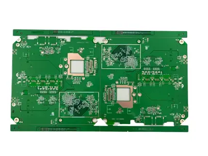
HDI board manufacturing is the fastest growing field in the printed circuit board industry. From the first 32-bit computer launched by HP in 1985 to today’s large-scale customer servers using 36 sequentially laminated multi-layer printed circuit boards and stacked micro-vias, HDI/micro-via technology is undoubtedly the future PCB architecture. Large ASICs and FPGAs with smaller device pitches,...

PCB Production Process: Subtractive and Additive Methods

Printed Circuit Boards (PCBs) are the foundation of modern electronic products, providing electrical connections and mechanical support for components. From consumer electronics and automotive systems to communication equipment and semiconductor applications, PCB manufacturing technology directly influences product performance, reliability, and production efficiency. During PCB fabrication, conductive patterns are created through different manufacturing approaches. The two...

HDI Board: High Density Interconnect Technology

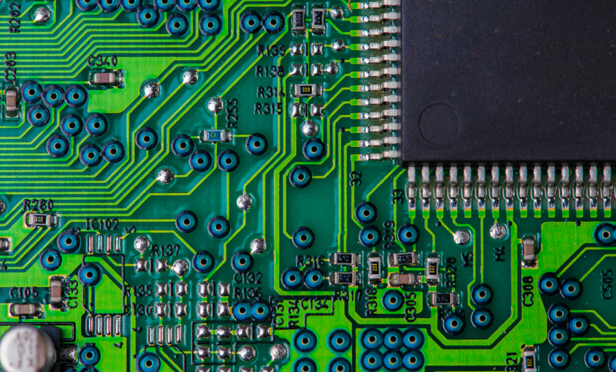
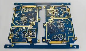
HDI boards, or High Density Interconnect boards, represent a significant advancement in PCB manufacturing, particularly suited for high-density circuit applications. These boards utilize micro-blind buried via technology to achieve compact designs with high line distribution density. Key characteristics include: Manufacturing Process: HDI boards typically employ micro-blind buried via technology, necessitating non-mechanical drilling methods such as laser...

Key Points of RF Circuit Board Design

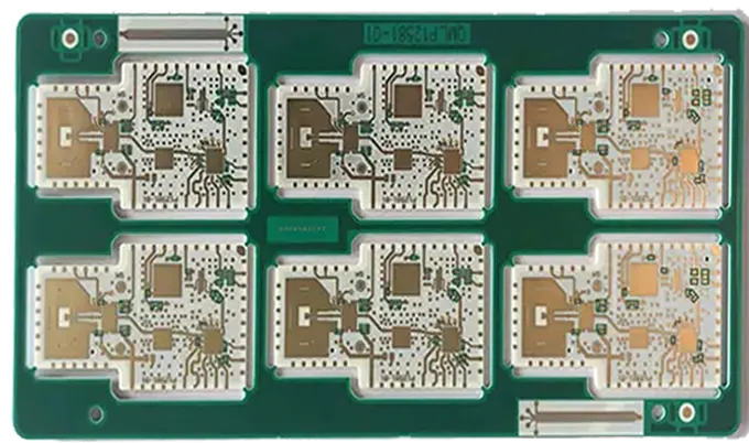
RF circuit board design is a critical and often complex area of PCB engineering. While there are many uncertainties in theory, practical design rules can be followed to optimize performance. The following key points will focus on RF circuit board partitioning and design strategies. 1. Microvias in RF Design Microvias are essential for connecting different layers on...

Practical Skills in High-Frequency PCB Design

In PCB design, achieving smaller, faster, and more cost-effective products is key. High-frequency PCB design presents unique challenges, especially at interconnection points, where electromagnetic properties must be carefully managed. This article focuses on practical skills for interconnection within the PCB board, providing valuable insights for engineers. For high-frequency applications, consider the following PCB design skills: Use 45° Transmission Line Corners:...

Copper Foil in PCB Laminates

The Complexity of Copper Foil in the PCB Industry Copper foil used in the PCB industry is more complex than one might imagine. Copper is not only an excellent electrical conductor but also a superb thermal conductor, making it the ideal material for most PCB applications. Understanding the various characteristics of copper foil is crucial for engineers....

Multilayer PCB Design Essentials

Multilayer PCB design follows principles similar to double-layer design, with added structural complexity and a focus on stable signal integrity and efficient routing. With experience in double-layer PCBs, moving to multilayer designs can be manageable. 1. Define the Layer Stack-Up Symmetry and Centering: Design the stack symmetrically around a central substrate layer for balance, and use...

Printed Circuit Board from design to production

In modern electronic systems, the Printed Circuit Board (PCB) serves as the foundation that connects and supports electronic components. From consumer electronics and communication equipment to automotive systems and medical devices, PCBs play a critical role in ensuring stable electrical performance, mechanical reliability, and long-term product functionality. A successful PCB requires more than just connecting...

High-frequency circuit wiring skills in PCB design

To ensure high-quality signal transmission and reliability in high-frequency PCB designs, adhering to effective wiring strategies is essential. Here are optimized guidelines and techniques, with key points highlighted for easy reference: 1. Minimize Interlayer Transitions Reducing the use of vias minimizes the interlayer transition effects and the distributed capacitance (about 0.5pF per via), improving speed and reducing...

Four Key Points in High-Speed PCB Design

When designing high-speed PCBs, process variations and other factors can significantly impact actual impedance. Automated design tools may not always detect these subtleties, making proactive, defensive design essential. Here’s how to address common challenges in high-speed PCB design. 1. Layer Stack-Up Configuration A well-configured layer stack-up is foundational for signal integrity (SI) and electromagnetic compatibility (EMC). Ideally,...