
Printed Circuit Boards (PCBs) are the foundation of modern electronic products, providing electrical connections and mechanical support for components. From consumer electronics and automotive systems to communication equipment and semiconductor applications, PCB manufacturing technology directly influences product performance, reliability, and production efficiency.
During PCB fabrication, conductive patterns are created through different manufacturing approaches. The two major PCB production methods are subtractive manufacturing and additive manufacturing.
The subtractive method has been widely used for decades and remains the dominant PCB manufacturing process. Meanwhile, additive manufacturing technologies are gaining attention due to increasing demand for miniaturization, high-density interconnects (HDI), and advanced electronic packaging.
Understanding the differences between these two processes helps engineers select suitable manufacturing solutions based on design complexity, performance requirements, and production goals.
1. Overview of PCB Pattern Formation Methods
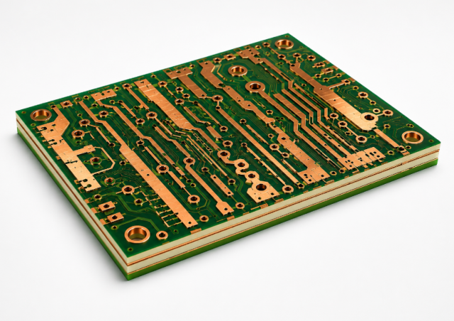
PCB production involves creating copper circuits on an insulating substrate. The main challenge is forming accurate conductive traces while maintaining electrical performance and mechanical reliability.
The two primary approaches are:
Subtractive Manufacturing
Subtractive manufacturing starts with a copper-clad laminate and removes unnecessary copper areas to create circuit patterns.
Additive Manufacturing
Additive manufacturing creates circuit patterns by selectively depositing copper onto the substrate surface.
The fundamental difference is:
- Subtractive process: Remove unwanted copper.
- Additive process: Build required copper structures.
2. Subtractive PCB Manufacturing Process
The subtractive process is the traditional and most widely adopted PCB fabrication method.
Basic Manufacturing Steps
1. Copper-Clad Laminate Preparation
PCB manufacturing begins with a laminate material consisting of:
- Insulating core material
- Copper foil layer(s)
Common substrate materials include:
- FR-4
- High-frequency laminates
- Polyimide materials
- Ceramic substrates
The copper layer serves as the starting conductive material.
2. Photoresist Coating
A photosensitive resist layer is applied to the copper surface.
This layer protects selected copper areas during the etching process.
3. Circuit Pattern Imaging
The desired circuit pattern is transferred onto the photoresist using:
- Photolithography
- Laser direct imaging (LDI)
The exposed areas define the final circuit layout.
4. Copper Etching
Chemical etching removes the unwanted copper from exposed areas.
After etching:
- Remaining copper forms circuit traces
- Removed areas become insulation gaps
5. Layer Alignment and Lamination
For multilayer PCBs:
- Inner layers are fabricated first
- Multiple layers are aligned
- Prepreg materials are added
- Layers are laminated under heat and pressure
This creates a complete multilayer PCB structure.
6. Drilling and Plating
Holes are drilled for:
- Component mounting
- Electrical connections between layers
Through-hole walls are plated with copper to create electrical connections.
Advantages of Subtractive Manufacturing
Mature and Reliable Technology
Subtractive PCB manufacturing has been developed for decades and has established production standards and quality control methods.
Suitable for Large-Scale Production
The process is highly optimized for mass production, making it cost-effective for many PCB applications.
Broad Material Compatibility
It supports various PCB materials and applications, including:
- Standard multilayer PCBs
- High-speed PCBs
- Automotive PCBs
- Industrial control boards
Limitations of Subtractive Manufacturing
Copper Waste
Since unnecessary copper is removed through etching, the process generates material waste.
Fine Pattern Limitations
As PCB designs become increasingly dense, traditional etching faces challenges in achieving extremely fine traces and spaces.
Reduced Efficiency for Advanced HDI Structures
Complex microvias and ultra-fine circuits may require additional advanced processes.
3. Additive PCB Manufacturing Process
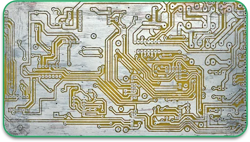
Additive manufacturing builds conductive structures by depositing copper only where circuits are required.
This approach is increasingly important for advanced PCB technologies.
Basic Manufacturing Steps
1. Substrate Preparation
The process begins with an insulating substrate surface.
The substrate may be:
- Organic laminate
- Flexible material
- Advanced packaging substrate
2. Circuit Pattern Formation
A pattern is created to define where copper will be deposited.
Common technologies include:
- Laser patterning
- Photolithography
- Masking processes
3. Copper Deposition
Copper is selectively deposited onto the designed areas through methods such as:
- Electroless copper plating
- Electroplating
- Direct copper deposition technologies
4. Additional Layer Building
Multiple conductive layers can be added sequentially to form complex structures.
This enables:
- Fine-line circuits
- High-density interconnects
- Advanced packaging designs
Types of Additive PCB Technologies
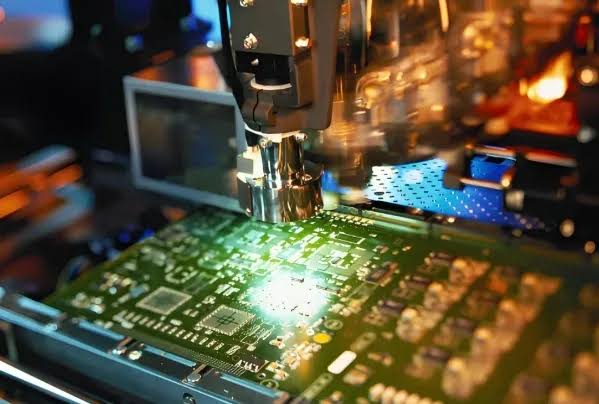
Semi-Additive Process (SAP)
Semi-additive manufacturing is widely used for advanced HDI and IC substrate applications.
The process typically includes:
- Applying a thin copper seed layer
- Patterning the circuit area
- Electroplating copper to build traces
- Removing unwanted seed copper
SAP enables finer line widths and spaces compared with traditional subtractive processes.
Fully Additive Process
Fully additive manufacturing deposits copper directly onto non-conductive substrates without requiring a copper foil starting layer.
Advantages include:
- Reduced copper waste
- High pattern accuracy
- Potential for advanced miniaturization
However, it requires more specialized materials and process control.
4. Subtractive vs. Additive PCB Manufacturing Comparison
| Comparison Factor | Subtractive Process | Additive Process |
|---|---|---|
| Manufacturing Principle | Remove unwanted copper | Add copper to create circuits |
| Technology Maturity | Very mature | Developing rapidly |
| Copper Utilization | More waste | Higher efficiency |
| Fine Line Capability | Moderate | Excellent |
| HDI Capability | Limited | Strong |
| Production Cost | Lower for standard PCBs | Higher for advanced applications |
| Process Complexity | Lower | Higher |
| Main Applications | Standard multilayer PCBs | HDI, IC substrates, advanced electronics |
5. Applications of Different PCB Manufacturing Methods
Subtractive Manufacturing Applications
Common applications include:
- Consumer electronics
- Industrial control systems
- Automotive control boards
- Communication equipment
- Power electronics
It remains the preferred choice for most conventional PCB production.
Additive Manufacturing Applications
Additive technologies are commonly used in:
- Semiconductor packaging
- High-density interconnect PCBs
- Miniaturized electronic devices
- Advanced mobile devices
- High-performance computing systems
- Wearable electronics
As electronic products continue becoming smaller and more powerful, additive manufacturing provides greater design flexibility.
6. Future Trends in PCB Manufacturing
The development of PCB manufacturing is moving toward higher density, improved reliability, and more environmentally friendly processes.
Future trends include:
Advanced HDI Manufacturing
Smaller vias, finer traces, and higher layer density will require more advanced additive technologies.
Improved Material Efficiency
Reducing copper waste and improving resource utilization will become increasingly important.
Integration with Semiconductor Technologies
PCB manufacturing and semiconductor packaging technologies are becoming increasingly interconnected.
Automated Process Control
AI-based inspection and intelligent manufacturing systems will further improve PCB production quality.
Conclusion
Both subtractive and additive manufacturing methods play important roles in PCB production.
The subtractive process remains the mainstream solution due to its maturity, reliability, and cost advantages, making it suitable for most conventional PCB applications.
The additive process, especially semi-additive technology, provides significant advantages in fine-line fabrication, HDI structures, and advanced electronic applications where miniaturization and high performance are critical.
Selecting the right PCB production method depends on factors such as design complexity, manufacturing requirements, cost considerations, and product performance goals. As electronic technologies continue to evolve, the combination of traditional and advanced PCB manufacturing methods will continue driving innovation in the electronics industry.





