
In modern electronic systems, the Printed Circuit Board (PCB) serves as the foundation that connects and supports electronic components. From consumer electronics and communication equipment to automotive systems and medical devices, PCBs play a critical role in ensuring stable electrical performance, mechanical reliability, and long-term product functionality.
A successful PCB requires more than just connecting components. It involves a comprehensive process covering schematic design, PCB layout, signal integrity optimization, manufacturing, inspection, and final assembly. Each stage directly affects the performance, reliability, and manufacturability of the final product.
What Is a Printed Circuit Board (PCB)?
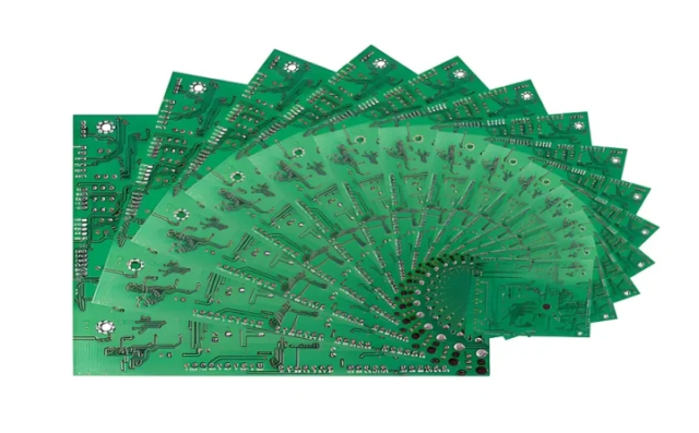
A Printed Circuit Board (PCB) is a structured electronic platform that mechanically supports components and electrically connects them through copper conductive traces.
A typical PCB consists of:
- Copper layers for electrical connections
- Dielectric materials for insulation
- Prepreg and core materials for multilayer structures
- Solder mask for protection
- Silkscreen markings for component identification
Common PCB substrate materials include FR-4, high-frequency laminates, metal-core materials, ceramic substrates, and flexible materials, depending on application requirements.
The PCB design process begins with understanding the product requirements, including:
- Electrical performance
- Mechanical dimensions
- Operating environment
- Thermal requirements
- Manufacturing constraints
These requirements determine the PCB structure, material selection, layer count, and layout strategy.
PCB Design Process
1. Schematic Design and Circuit Planning
The PCB development process begins with schematic capture.
Engineers use electronic design automation (EDA) tools to create a circuit diagram that defines:
- Component connections
- Signal flow
- Power distribution
- Interface requirements
The schematic acts as the electrical blueprint of the PCB and provides the foundation for the physical layout.
During this stage, engineers evaluate:
- Component selection
- Power requirements
- Signal classification
- Design constraints
A well-developed schematic reduces design risks in later PCB layout stages.
2. PCB Library Development
Before layout begins, engineers create and verify PCB component libraries.
A complete PCB library typically includes:
- Schematic symbols
- PCB footprints
- 3D models
- Simulation models
- Manufacturing information
Accurate library development is essential because incorrect footprints or component dimensions can lead to:
- Assembly issues
- Component misalignment
- Manufacturing delays
A reliable component library improves design efficiency and ensures compatibility between design and production.
3. PCB Layout and Routing
PCB layout converts the electrical schematic into a physical circuit structure.
During component placement, engineers consider:
- Signal flow optimization
- Thermal distribution
- Mechanical constraints
- Assembly requirements
- Manufacturing feasibility
Critical components such as processors, RF devices, power modules, and connectors require careful placement to minimize signal loss and improve system reliability.
High-Speed PCB Routing Considerations
For high-speed and high-frequency applications, routing quality directly affects performance.
Engineers must control:
- Trace impedance
- Differential pair matching
- Signal return paths
- Crosstalk
- Electromagnetic interference (EMI)
Common optimization methods include:
- Controlled impedance design
- Proper layer stackup planning
- Ground plane optimization
- Short and direct signal paths
Simulation tools such as Signal Integrity (SI) and Power Integrity (PI) analysis help identify potential issues before manufacturing.
PCB Manufacturing Process
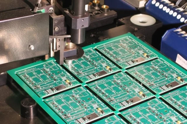
After design approval, PCB fabrication begins. A typical PCB manufacturing process includes multiple precision-controlled steps.
1. Inner Layer Fabrication
For multilayer PCBs, inner layers are manufactured first.
The process includes:
- Copper imaging
- Etching
- Automated Optical Inspection (AOI)
- Oxide treatment
The goal is to create accurate internal circuits with reliable layer alignment
2. Lamination
Multiple PCB layers are bonded together through a controlled lamination process.
Key factors include:
- Temperature control
- Pressure control
- Material compatibility
- Layer registration accuracy
Proper lamination ensures mechanical strength and prevents defects such as:
- Delamination
- Voids
- Warpage
3. Drilling and Plating
After lamination, mechanical drilling or laser drilling creates electrical connections between layers.
Common via structures include:
- Through vias
- Blind vias
- Buried vias
- Microvias
Copper plating is then applied to establish reliable electrical connections.
Precision drilling and plating are especially important for HDI, fine-pitch, and high-frequency PCB applications.
4. Surface Finishing and Protection
Surface finishing protects exposed copper and improves solderability.
Common finishes include:
- ENIG
- ENEPIG
- HASL
- OSP
The solder mask layer protects circuits from oxidation and prevents solder bridging during assembly.
PCB Testing and Quality Control
Before assembly, fabricated PCBs undergo strict inspection and electrical testing.
Common inspection methods include:
Automated Optical Inspection (AOI)
AOI verifies:
- Trace defects
- Missing circuits
- Short circuits
- Layer alignment issues
Electrical Testing (E-Test)
Electrical testing checks:
- Continuity
- Insulation resistance
- Open and short circuits
For high-reliability applications, additional validation may include:
- Impedance testing
- Thermal cycling
- Reliability testing
- Environmental testing
These processes ensure PCB performance meets customer and industry requirements.
PCB Assembly and Final Validation
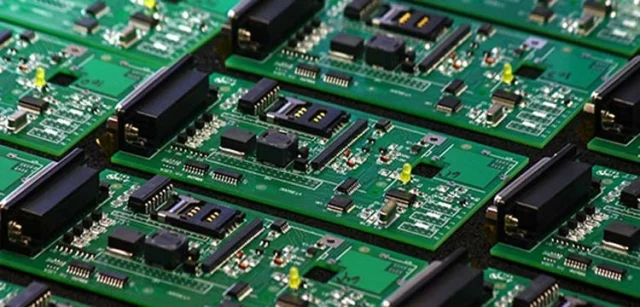
After PCB fabrication and testing, components are assembled onto the board.
The main assembly technologies include:
Surface Mount Technology (SMT)
SMT enables:
- High-density component placement
- Compact PCB designs
- Automated mass production
Through-Hole Technology (THT)
THT provides:
- Strong mechanical connections
- High-current capability
- Reliable connections for large components
After assembly, PCBAs undergo final inspection and testing, including:
- AOI inspection
- X-ray inspection
- Functional testing
- Thermal and environmental validation
Importance of PCB Design and Manufacturing Integration
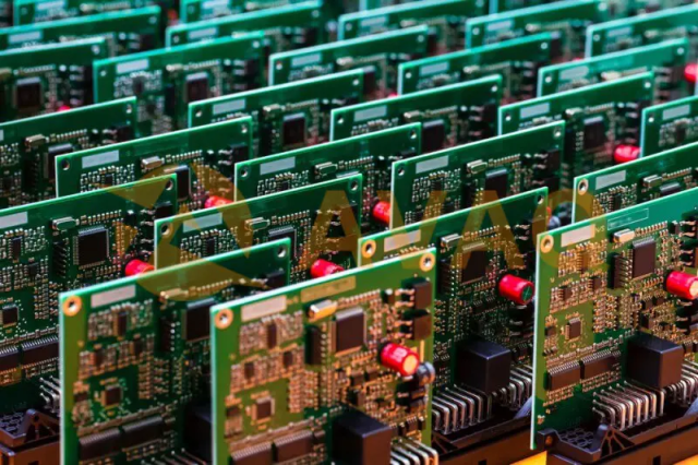
A high-quality PCB requires close cooperation between design and manufacturing teams.
Design decisions influence:
- Production yield
- Assembly efficiency
- Cost control
- Long-term reliability
Design for Manufacturability (DFM) analysis helps identify potential risks early, including:
- Difficult routing structures
- Insufficient spacing
- Component placement issues
- Manufacturing limitations
Early engineering collaboration reduces redesign cycles and accelerates time to market.
Conclusion
The journey of a Printed Circuit Board from schematic design to final production involves multiple engineering disciplines, including circuit design, PCB layout, material selection, fabrication, assembly, and testing.
As electronic products continue to demand higher performance, smaller form factors, and greater reliability, advanced PCB technologies and manufacturing expertise become increasingly important.
At KKPCB, we provide comprehensive PCB and PCBA solutions covering PCB fabrication, engineering support, component sourcing, and assembly services. Through DFM analysis, advanced manufacturing processes, and strict quality control, we help customers transform PCB designs into reliable production-ready products.





