
HomeTag

RF connector launch - KKPCB

Ku/Ka Satellite PCB Launch Design: Taming Connector and Via Transitions at 30 GHz

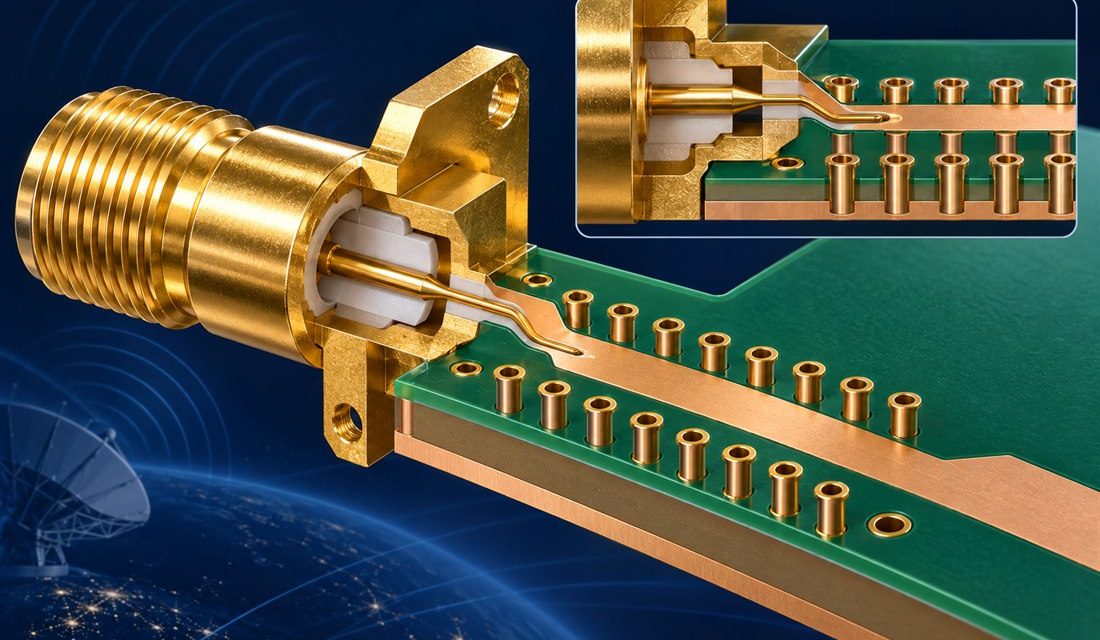
For Satellite PCB launch design, a Ku/Ka payload can meet its schematic targets and still lose margin at the board edge. The connector, launch pad, reference plane, via field, and enclosure datum form one electromagnetic interface. The Satellite PCB release must hold that board-to-enclosure datum constant across design and manufacturing. At 30 GHz, even a...
Duroid 5880 PCB Connector Launch: 8 Critical Controls for Repeatable RF Assembly

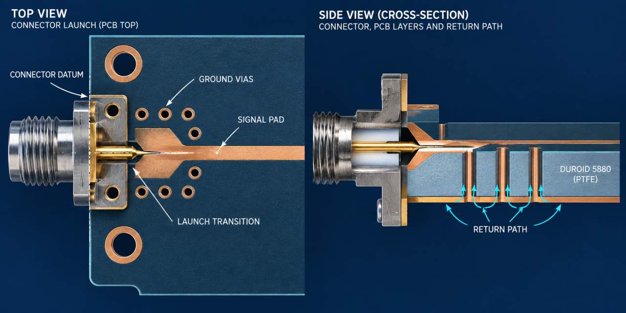
Contents Why the connector launch controls RF yield Layout and datum controls Assembly and inspection controls Release checklist Duroid 5880 PCB connector launches are a common project pain point. A layout can meet the simulated impedance target and still show return-loss variation when the connector datum, plated holes, solder fillet, or ground-via pattern changes during...