HomeTag

PCB warpage - KKPCB

PCB Warpage: Causes, Prevention & Solutions Explained

In PCB manufacturing and assembly, dimensional stability is a critical factor that directly affects product reliability and production yield. One common but often underestimated challenge is PCB warpage. PCB warpage occurs when a circuit board bends, twists, or loses its original flatness due to thermal stress, material characteristics, design imbalance, or manufacturing process variations. Although...
Common Problems and Solutions for Substrates in PCB Design

In modern PCB design, the choice and handling of substrate materials play a critical role in determining the overall performance, reliability, and manufacturability of the circuit board. Substrate-related issues can lead to serious defects such as poor solderability, delamination, signal loss, and even complete product failure. This article outlines the most common substrate problems encountered...

What is PCB warpage?

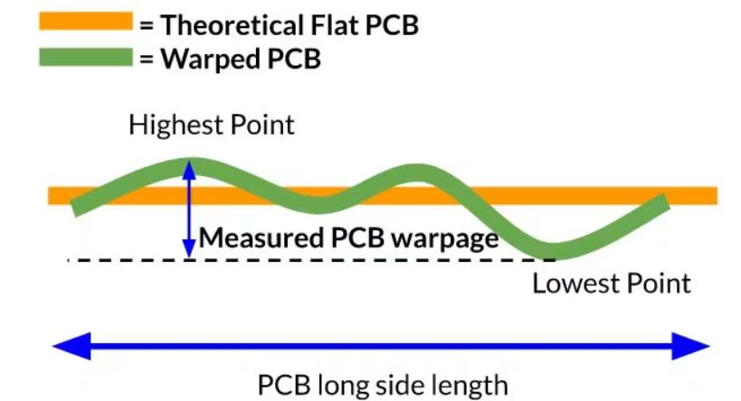
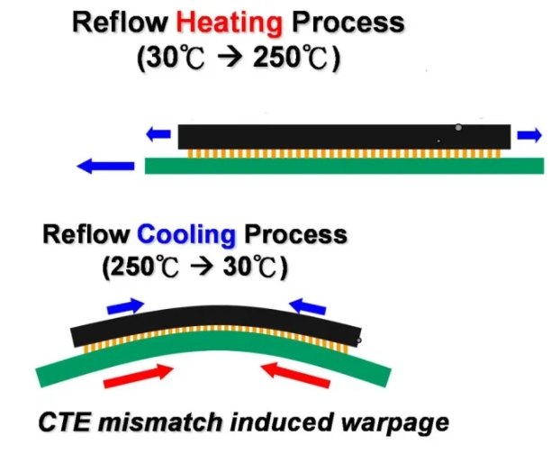
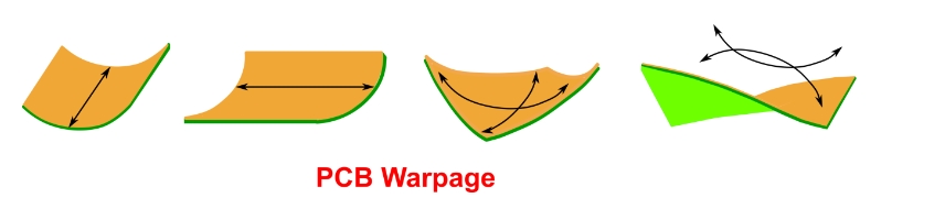
What is PCB Warpage? PCB warpage refers to the unwanted bending, twisting, or deformation of a printed circuit board from its intended flat shape. Ideally, a PCB should maintain a flat and stable surface throughout fabrication, assembly, and operation. However, differences in material properties, thermal expansion, copper distribution, and manufacturing processes can cause the PCB...

How to Check for PCB Warpage: Techniques and Methods

How to Check for PCB Warpage: Techniques and Methods PCB warpage (also known as bow and twist) is a common manufacturing defect that occurs when a printed circuit board deviates from perfect flatness. It can lead to serious issues during SMT assembly, such as poor solder joint formation, component misalignment, open circuits, or bridging. In...