PCB Stack-Up Design - KKPCB
 
HomeTag

PCB Stack-Up Design - KKPCB

Low Loss PCB: Materials, Design Principles, and High-Frequency Performance Optimization

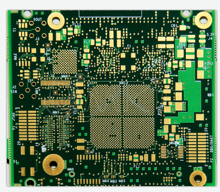
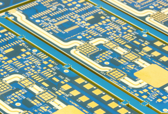
1. Introduction: Why Low Loss PCB Is Essential in Modern Electronics As electronic systems evolve toward: Higher data rates Higher operating frequencies Increased signal density Greater system integration traditional PCB materials such as standard FR4 are no longer sufficient for advanced RF and high-speed applications. In modern systems including: 5G/6G communication networks Automotive radar systems...

HDI PCBs Explained: Stack-Up Choices, Via Strategies, and Cost Trade-Offs

What Actually Defines an HDI PCB? An HDI PCB (High-Density Interconnect PCB) is not defined by layer count alone, but by how efficiently interconnections are implemented. The key differentiators are: Microvias (laser-drilled vias) Blind and buried vias Fine line and spacing (typically ≤100 µm) High connection density per unit area The goal of HDI is...