1. Introduction: Why Low Loss PCB Is Essential in Modern Electronics
As electronic systems evolve toward:
- Higher data rates
- Higher operating frequencies
- Increased signal density
- Greater system integration
traditional PCB materials such as standard FR4 are no longer sufficient for advanced RF and high-speed applications.
In modern systems including:
- 5G/6G communication networks
- Automotive radar systems
- Satellite communication modules
- High-speed computing and servers
- Microwave and RF electronics
Low Loss PCB technology is essential to ensure stable and efficient signal transmission.
At KKPCB, low loss PCB solutions are engineered for minimal signal attenuation, stable impedance, and high-frequency reliability.
2. What Is a Low Loss PCB?
A Low Loss PCB is a printed circuit board designed using materials and structures that minimize signal energy loss during transmission.
Signal loss in PCB systems is mainly caused by:
- Dielectric loss in the substrate material
- Conductor loss in copper traces
- Surface roughness effects
- Impedance discontinuities
Low loss PCB technology focuses on reducing all these factors to maintain:
- Signal strength
- Transmission efficiency
- High-frequency stability
3. Key Characteristics of Low Loss PCB Materials
3.1 Low Dielectric Loss
The dielectric loss behavior is described by:
tanδ\tan\deltatanδ
A lower loss tangent means:
- Less signal energy dissipation
- Better RF efficiency
- Improved high-frequency performance
3.2 Stable Dielectric Constant
Low loss materials maintain:
- Consistent impedance
- Stable phase performance
- Predictable signal propagation
3.3 High-Frequency Signal Integrity
Low loss PCBs support:
- Reduced insertion loss
- Minimal signal distortion
- Stable high-speed transmission
4. Common Low Loss PCB Materials
4.1 PTFE-Based Laminates
Widely used in RF and microwave applications:
- Extremely low dielectric loss
- Excellent high-frequency stability
4.2 Rogers High-Frequency Materials
Such as:
- RO4350B
- RO4003C
- RT/duroid® series
These materials provide:
- Balanced performance and manufacturability
- Low insertion loss
- Stable electrical properties
4.3 Advanced Hydrocarbon and LCP Materials
Used in:
- High-speed digital systems
- Compact RF modules
- mmWave applications
5. Why Low Loss PCB Matters in High-Frequency Design
At high frequencies, signal loss becomes a critical performance limiter.
Key benefits of low loss PCB include:
- Longer signal transmission distance
- Higher data throughput
- Improved RF efficiency
- Reduced power consumption
Maintaining controlled impedance ensures:
- Reduced signal reflection
- Stable waveform integrity
- Better system reliability
6. Low Loss PCB Design Considerations
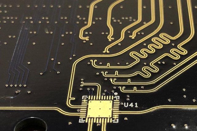
6.1 Transmission Line Optimization
Key routing strategies:
- Controlled impedance traces
- Short signal paths
- Minimized vias in RF paths
6.2 Stack-Up Design
A well-designed PCB stack-up ensures:
- Stable dielectric spacing
- Consistent impedance
- Reduced EMI coupling
6.3 Copper Surface Roughness Control
Copper roughness directly impacts:
- High-frequency attenuation
- Signal propagation loss
Low-profile copper improves:
- RF performance
- Signal efficiency
6.4 Differential Pair Routing
Used in high-speed systems:
- USB
- PCIe
- Ethernet
Benefits:
- Reduced noise
- Improved signal integrity
- Better EMI performance
7. Thermal Performance in Low Loss PCB
Although focused on electrical performance, thermal stability is also critical.
Low loss PCB systems must handle:
- Power dissipation
- RF heating effects
- Long-term operational stress
Thermal management methods include:
- Thermal via arrays
- Copper heat spreading planes
- Metal-backed structures in high-power designs
At KKPCB, thermal and RF design are integrated for optimal performance.
8. Manufacturing Challenges of Low Loss PCB
8.1 Material Processing Complexity
Low loss materials such as PTFE require:
- Specialized lamination processes
- Precise drilling control
- Stable bonding techniques
8.2 Tight Impedance Tolerance
Manufacturing must ensure:
- Consistent trace width
- Accurate dielectric thickness
- Controlled copper etching
8.3 High-Frequency Quality Control
Testing includes:
- TDR impedance testing
- RF signal integrity validation
- Loss measurement analysis
9. Applications of Low Loss PCB

Low loss PCBs are widely used in:
- 5G and 6G communication systems
- Automotive radar (ADAS systems)
- Satellite communication modules
- RF amplifiers and transceivers
- Microwave sensing systems
- High-speed computing infrastructure
These systems require:
- High signal accuracy
- Low transmission loss
- Stable high-frequency performance
10. Future Trends in Low Loss PCB Technology
Future developments focus on:
- Sub-THz communication systems
- Ultra-low loss dielectric materials
- Integrated RF and antenna modules
- Advanced hybrid stack-up structures
- High-density RF integration
Low loss PCB technology will continue to evolve to support:
- Higher frequencies
- Greater bandwidth
- More compact system architectures
11. Conclusion
Low Loss PCB technology is a cornerstone of modern high-frequency and high-speed electronic systems.
By minimizing signal attenuation and improving impedance stability, it enables:
- Reliable RF communication
- High-speed data transmission
- Efficient power usage
With advanced material selection and precision manufacturing expertise, KKPCB delivers high-performance PCB solutions for next-generation electronic systems.
