HomeTag

PCB manufacturing - KKPCB

PCB Factory Direct: Cost-Effective and Reliable PCB Manufacturing from the Source

In today’s global electronics supply chain, many companies are choosing PCB factory direct sourcing to reduce costs, improve communication, and ensure consistent manufacturing quality. Working directly with a PCB factory eliminates unnecessary intermediaries and gives customers greater control over pricing, lead time, and production transparency. This article explains what PCB factory direct means, why it...
PCB Price Request: What Information You Need for an Accurate and Fast Quotation

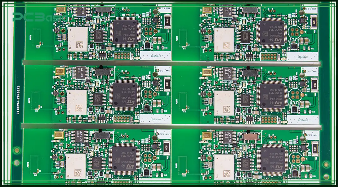
Submitting a clear and complete PCB price request is the first step toward accurate pricing, short lead times, and smooth production. Whether you are sourcing prototype PCBs, small batch orders, or mass production, providing the right information helps PCB manufacturers evaluate cost, manufacturability, and delivery schedules efficiently. This article outlines the essential details required for...

Buy High Frequency PCBs Using Rogers, PTFE, and Hybrid Stackups for High-Speed RF Front-End Modules

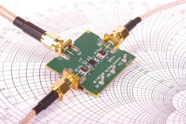
Engineering Context As wireless communication technologies evolve toward 5G Advanced, Wi-Fi 7, satellite communications, and mmWave radar, RF front-end modules have become increasingly complex. Modern RF front-end architectures integrate power amplifiers (PAs), low-noise amplifiers (LNAs), filters, switches, duplexers, and antenna arrays into compact, multilayer PCB assemblies that demand exceptional electrical performance. For OEMs and procurement...

Accelerate Product Validation and Engineering Iteration with High-Reliability Small Batch PCB Manufacturing

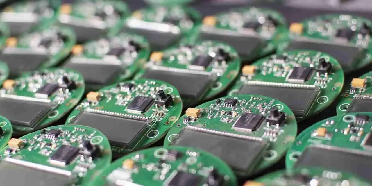
In today’s highly competitive electronics market, speed and reliability are critical during the product development stage. High-reliability small batch PCB manufacturing enables engineers to accelerate product validation, shorten engineering iteration cycles, and reduce development risk before mass production. This article explains how small batch PCB manufacturing supports rapid prototyping, design verification, and engineering optimization, helping...

PCB Turnkey Services: A Complete One-Stop Solution for PCB Manufacturing and Assembly

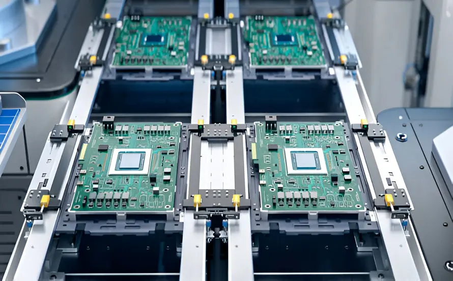
Engineering Context As electronic products become increasingly complex, managing multiple suppliers for PCB fabrication, electronic components, SMT assembly, testing, and logistics introduces significant risks to project schedules, product quality, and overall cost. Communication gaps between suppliers often result in engineering inconsistencies, sourcing delays, production defects, and extended time-to-market. PCB Turnkey Services provide a comprehensive manufacturing...

Impedance Control on PCBs: Why It Matters for High-Speed, RF, and High-Frequency Circuit Design

As electronic devices continue to evolve toward higher speeds, greater bandwidth, and higher operating frequencies, impedance control on PCBs has become a critical requirement rather than an optional design consideration. In high-speed PCB, RF PCB, and high-frequency circuit design, improper impedance control can lead to signal degradation, EMI issues, and overall system instability. This article...

Key Manufacturing Factors That Affect Controlled Impedance PCB Accuracy

Key Manufacturing Factors That Affect Controlled Impedance PCB Accuracy In today’s high-speed electronics market, Controlled Impedance PCB manufacturing has become a fundamental requirement for ensuring excellent signal integrity and stable electrical performance. As operating frequencies and data transmission speeds continue to rise, even minor impedance deviations in a controlled impedance PCB can result in signal...

Control of Conductor Etching in PCB Manufacturing: Precision Copper Etching for Fine-Line Circuit Patterns

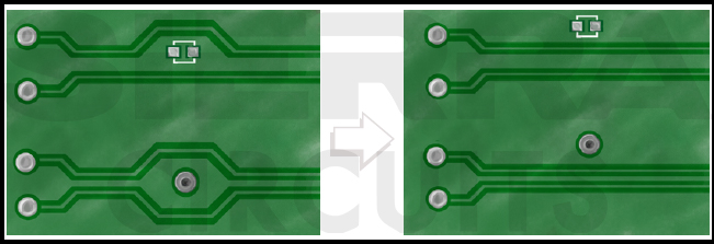
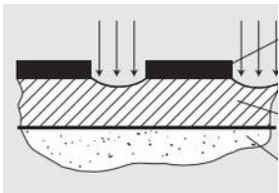
Control of Conductor Etching Process in Printed Circuit Boards Copper etching is one of the most critical steps in printed circuit board (PCB) manufacturing, as it directly determines the accuracy and reliability of conductive circuit patterns. The term “printed circuit board” originates from this process, since etching is the final stage of photolithography used to...

Achieve Low-Loss Transmission and Stable Impedance Performance with Double Layer HF PCB Engineering for High-Frequency Communication Systems

A Double Layer HF PCB may appear structurally simple, yet in high-frequency engineering it provides a remarkably efficient platform for low-loss propagation, stable impedance, and predictable electromagnetic behavior. When RF designers need high-frequency stability without the cost or stackup escalation of multilayer PCBs, a Double Layer HF PCB offers the ideal balance between manufacturability and...

PCB Prototype Engineering: Achieving High Reliability, High Speed, and High Precision in Modern Electronics

Introduction: Why PCB Prototype Engineering Defines Modern Electronics A PCB Prototype is no longer just a pre-production sample—it is the central engineering stage that determines product performance, manufacturability, reliability, and cost.In advanced electronics such as 5G, IoT, robotics, automotive, aerospace, AI edge computing, and industrial automation, a well-engineered PCB Prototype ensures signal integrity, thermal stability,...