HomeTag

multilayer PCB - KKPCB

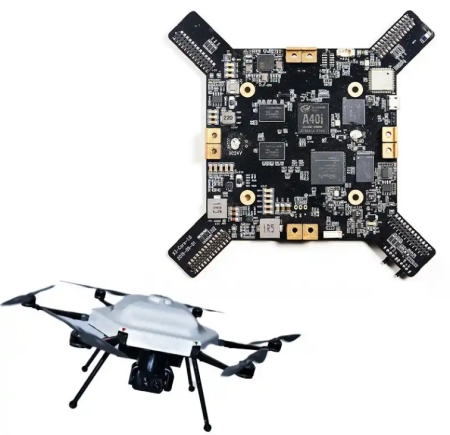
UAV PCB: High-Reliability Circuit Boards for Unmanned Aerial Vehicle Systems

Unmanned Aerial Vehicles (UAVs), commonly known as drones, rely on advanced electronic systems to perform navigation, communication, imaging, and flight control functions. At the core of these systems is the UAV PCB, which integrates critical electronic components to ensure stable operation, lightweight design, and high reliability during flight. UAV PCBs must operate under demanding conditions...
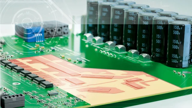
Low Loss PCB: High-Performance Circuit Boards for High-Speed and RF Applications

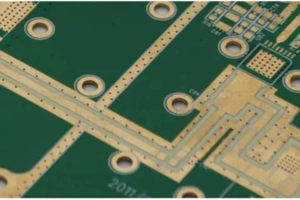
As modern electronic systems continue to operate at higher frequencies and faster data rates, signal integrity has become a critical factor in PCB design. Low Loss PCB technology is specifically developed to reduce signal attenuation and maintain high signal quality in high-speed digital and RF applications. Low loss PCBs use specialized dielectric materials that minimize...

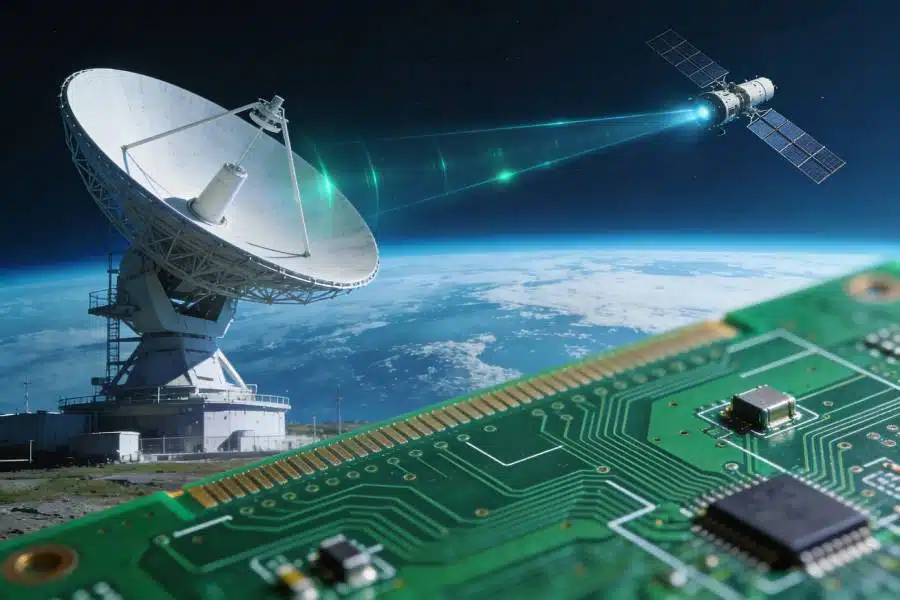
Satellite PCB: High-Reliability Circuit Boards for Space and Satellite Communication Systems

Introduction to Satellite PCB Satellite communication and space technologies require electronic systems that can operate reliably in extreme environments such as vacuum, radiation exposure, and large temperature variations. A Satellite PCB is a high-reliability printed circuit board designed specifically for spacecraft electronics and satellite communication systems. These PCBs support critical subsystems including communication modules, navigation...

High Layer Count PCB: Advanced Multilayer PCB Design for Complex Electronics

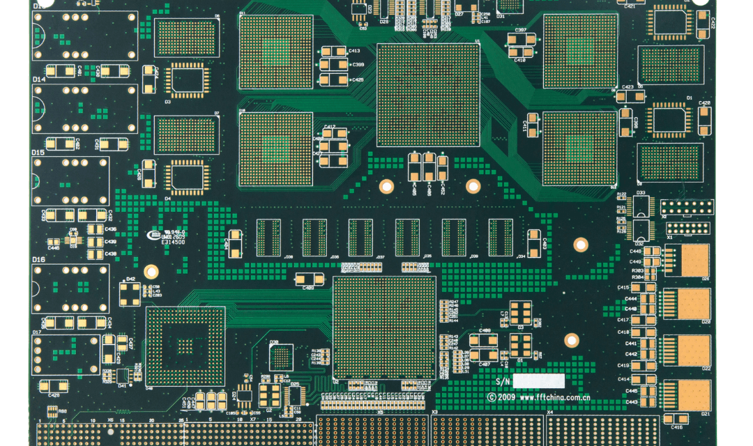
As electronic systems become more powerful and complex, standard multilayer PCBs are sometimes no longer sufficient. Advanced applications such as telecommunications infrastructure, data servers, and aerospace electronics often require extremely dense routing and precise signal control. This is where High Layer Count PCBs come into play. These circuit boards typically contain 20 layers or more,...

Buried Via PCB: Advanced PCB Design for High-Density and High-Speed Electronics

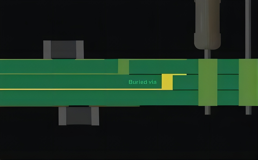
As electronic devices become smaller and more powerful, PCB designers face a constant challenge: fitting more circuitry into less space. Traditional through-hole vias can quickly consume valuable routing area, especially in multilayer boards. This is where Buried Via PCB technology becomes extremely useful. By placing vias entirely within internal layers, designers can maximize routing space...

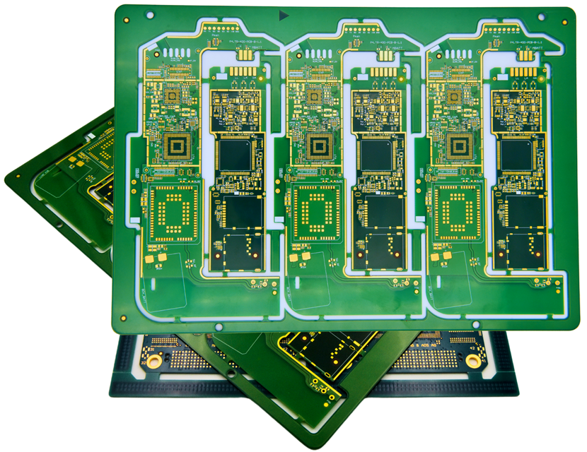
Multilayer PCB: Advanced Design for High-Density and High-Speed Electronics

Multilayer PCB: Advanced Design for High-Density and High-Speed Electronics With modern electronic devices becoming increasingly compact and high-performance, Multilayer PCB technology is essential for achieving complex circuit routing, improved signal integrity, and efficient power distribution. A multilayer PCB consists of three or more conductive copper layers laminated together with dielectric materials , enabling compact, high-density,...

Microvia PCB: High-Density Interconnect Solutions for Advanced Electronics

Microvia PCB: High-Density Interconnect Solutions for Advanced Electronics As electronic devices become smaller, faster, and more complex, designers face increasing challenges in routing high-density circuits. Microvia PCB technology provides a solution by enabling high-density interconnects (HDI), allowing for compact multilayer designs with superior electrical performance. A Microvia PCB uses extremely small vias, typically less than...

BT Epoxy PCB: Enhancing Reliability in Modern Multilayer Electronics

As electronics continue to evolve, demands for high-performance, multilayer PCBs have surged. BT Epoxy PCBs (Bismaleimide-Triazine epoxy boards) have become a preferred choice for designers who need robust thermal, mechanical, and electrical performance in demanding applications. Unlike conventional FR4 boards, BT Epoxy offers superior dimensional stability, low thermal expansion, and high glass transition temperature (Tg)—critical...

Why Multilayer PCBs Are Essential for High-Speed and High-Density Electronics

As electronic devices continue to evolve toward higher performance and smaller form factors, traditional two-layer circuit boards are no longer sufficient for many modern applications. This is where multilayer PCBs play a crucial role. By integrating multiple conductive layers into a single compact structure, multilayer PCBs enable engineers to design complex circuits while maintaining signal...

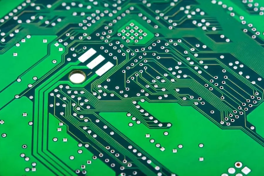
Buried Via PCB – Advanced Multilayer PCB Technology for High-Density Circuit Design

What Is a Buried Via PCB? A Buried Via PCB is a type of multilayer printed circuit board that uses buried vias to connect internal copper layers without reaching the outer surface layers. Unlike through-hole vias that pass through the entire board, buried vias exist only between inner layers, remaining invisible from the exterior of...