low-loss PCB - KKPCB
 
HomeTag

low-loss PCB - KKPCB

Optimize Thermal Performance and EMI Suppression in High-Density RF Modules with Low Loss PCB Materials

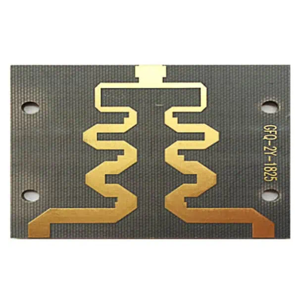
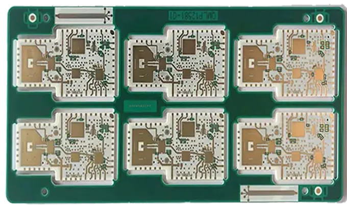
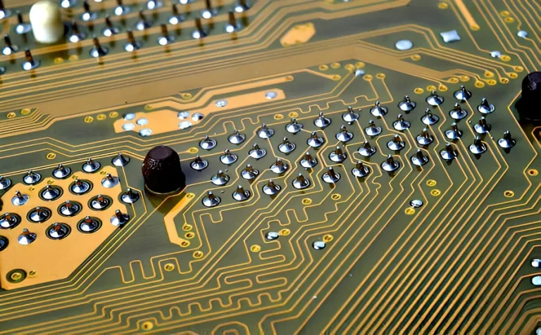
High-density RF modules used in 5G radios, SATCOM terminals, phased-array beamformers, and mmWave front-end units are increasingly constrained by thermal stress, EMI coupling, and insertion loss. As operating frequencies push beyond 10–40 GHz, traditional FR-4 structures can no longer maintain stable impedance, consistent dielectric behavior, or low-loss routing. This is where Low Loss PCB materials—such...

mmWave Module PCB Engineering for High-Frequency, Low-Loss and Thermally Stable RF Front-End Systems

The shift toward 5G FR2, advanced radar, high-resolution sensing and satellite communication has placed intense performance pressure on mmWave Module PCB design. At frequencies from 24 GHz to 86 GHz, the PCB is no longer a passive carrier—it becomes an active RF component whose materials, stackup, via transitions and routing geometries directly dictate performance. A...

Reduce Insertion Loss and Enhance Power Efficiency Using Low Loss PCB Designs for Satellite Communication Payloads

Satellite communication payloads demand high-frequency RF stability, minimal insertion loss, and optimized power efficiency across densely packed multilayer PCBs. Signal integrity degradation, EMI coupling, or thermal hotspots can compromise link margin, telemetry accuracy, and antenna performance. Low loss PCB materials, such as ceramic-reinforced laminates or PTFE-based RF substrates, provide stable dielectric constant (Dk) and low...

Minimize Crosstalk and Maintain Impedance Precision Using Advanced Blind Via PCB Layouts in 5G mmWave Systems

5G mmWave hardware doesn’t leave much room for layout mistakes. When operating above 24 GHz, a few microns of misalignment, a poorly shaped via stub, or an uncontrolled dielectric transition can collapse RF integrity. That is why advanced blind via PCB layouts have become a core enabling technology for minimizing crosstalk, stabilizing impedance, and preserving...

Enhance Signal Accuracy and Low-Noise Stability with High Frequency Sensor PCB Platforms for Industrial IoT Detection Systems

Industrial IoT detection systems rely on a dense network of sensors for accurate monitoring of environmental parameters, machinery status, and process analytics. High frequency sensor PCBs must maintain low insertion loss, high signal-to-noise ratio, and phase-stable routing across multiple sensor channels to ensure reliable data acquisition. High frequency sensor PCB laminates (Dk = 3.2 ±...

Optimize High-Frequency UAV PCB Architectures to Enhance IoT Crop Monitoring, Precision Spraying, and Long-Range Agricultural Drone Communication

IoT-enabled agricultural UAVs operate in a uniquely demanding environment: wide temperature swings, continuous vibration, variable humidity, and rapidly changing RF propagation conditions over open farmland. These drones must maintain long-range wireless links, collect high-resolution crop data, and execute precision-controlled spraying while keeping power consumption and mass as low as possible. To meet these requirements, modern...

Boost RF Linearity and Phase Consistency with Impedance Controlled PCB Architectures in Aerospace Navigation and Telemetry Modules

Aerospace navigation and telemetry links depend on signals that simply cannot drift, distort, or wander off-phase. Whether guiding a launch vehicle or stabilizing a satellite’s inter-orbital communication, the RF path must maintain tight impedance control, predictable phase behavior, and ultra-low distortion across multi-GHz carriers. This is where Impedance Controlled PCB architectures become fundamental—not an optional...

Achieve Low-Loss Performance and Long-Term Stability Through ADAS PCB Materials for Multi-Sensor Fusion Modules

Advanced driver-assistance systems (ADAS) rely heavily on multi-sensor fusion, where radar, LiDAR, ultrasonic sensing, and camera modules continuously exchange high-frequency data. To maintain real-time performance and safety-critical reliability, the ADAS PCB must deliver low-loss signal transmission, stable dielectric behavior, and tight impedance control under prolonged automotive thermal and vibration stress. High-frequency ADAS RF chains—particularly 24...

Optimize Signal Integrity and Multi-Band RF Stability with 5G Router PCB Architectures Using Low-Loss Materials

Next-generation 5G routers operate across 2.4, 5, and 6 GHz bands while supporting high-speed MIMO data streams and concurrent RF channels. Maintaining signal integrity, low insertion loss, and impedance accuracy across multilayer PCB architectures is critical for throughput, link stability, and network reliability. Low-loss PCB laminates (Dk ~3.0 ±0.04, Df ~0.0012 @10 GHz) provide minimal...

Drive Ultra-Clean Electromagnetic Performance Through Precision-Aligned Multilayer HF PCB Dielectrics in Wideband Radar Processing Units

Wideband radar processing units operating in 8–40 GHz and beyond require multilayer HF PCBs with precisely aligned dielectric layers to maintain ultra-clean electromagnetic performance. Signal integrity, insertion loss, and phase stability are critically sensitive to stackup alignment, trace spacing, and dielectric uniformity. KKPCB leverages precision-laminated multilayer HF PCB substrates, low-roughness copper, and impedance-calibrated routing to...