HDI PCB Design - KKPCB
 
HomeTag

HDI PCB Design - KKPCB

Impedance Matching in HDI PCB Design

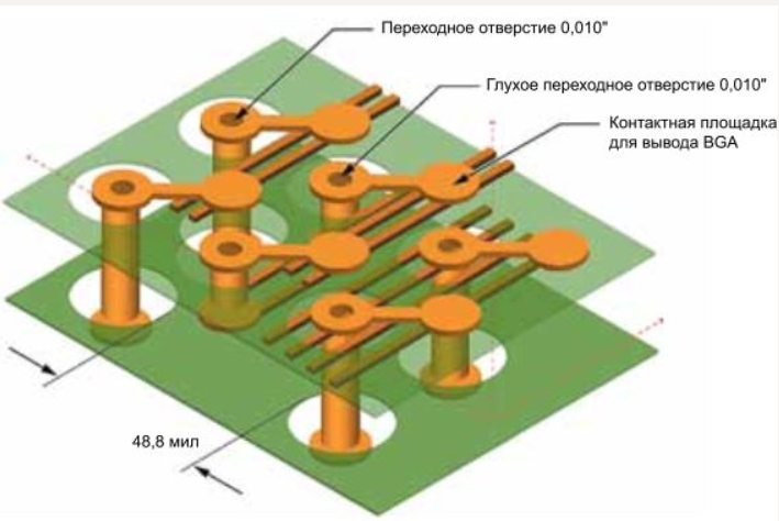
In modern HDI PCB design (High-Density Interconnect PCB design), achieving precise impedance matching is essential for maintaining signal integrity, minimizing reflection, and ensuring high-speed signal transmission. As data rates increase and circuit density grows, impedance control in HDI PCB layout becomes more complex due to fine trace geometries, microvias, and multilayer stack-ups. Effective impedance matching...

Impedance Matching in HDI PCB Design

Impedance matching in HDI ( High- Density Interconnect ) boards is intended to prevent transmission errors, especially losses caused by transmission line resistance and the dielectric properties of the printed circuit board. Microvias can be used to create manufacturing-friendly PCB layouts in impedance-matched systems. BGA escape routing and dogbone fanout structures enable impedance matching in HDI PCBs. When do PCB traces...

BGA Assembly: Beginner’s Guide to Ball Grid Array Assembly

Why BGA Assembly Is Critical in Modern PCB Design As electronic devices move toward miniaturization, high-speed performance, and high pin-count integration, the Ball Grid Array (BGA) assembly has become a mainstream packaging technology in: Microprocessors (CPU/GPU) FPGAs High-speed communication ICs Memory devices (DDR, LPDDR) Compared with traditional packages (QFP, SOP), BGA offers: Higher I/O density...

Multilayer PCB Manufacturing Process, Advantages and Applications

1. Introduction: Why Multilayer PCBs Are Essential in Modern Electronics As electronic devices continue to evolve toward miniaturization, high-speed performance, and multifunction integration, traditional single-layer or double-layer PCBs can no longer meet design requirements. This has led to the widespread adoption of multilayer PCBs (Multilayer Printed Circuit Boards), which integrate multiple conductive layers within a...

Ball Grid Array (BGA) Package

The Ball Grid Array (BGA) package is one of the most widely used advanced semiconductor packaging technologies in modern high-density PCB design and PCBA assembly. It is designed to provide high pin-count interconnections, improved electrical performance, and enhanced thermal management compared to traditional packages such as QFP or QFN. BGAs are extensively used in CPU,...

Advanced PCB Footprint Generator: Key to Efficient PCB Design

1. Introduction: Why PCB Footprint Accuracy Matters in Modern Electronics In modern PCB design and electronic product development, accuracy at the earliest design stage directly determines manufacturing success, cost efficiency, and product reliability. One of the most critical elements in PCB layout design is the PCB footprint, which defines the physical land pattern for electronic...