The Ball Grid Array (BGA) package is one of the most widely used advanced semiconductor packaging technologies in modern high-density PCB design and PCBA assembly. It is designed to provide high pin-count interconnections, improved electrical performance, and enhanced thermal management compared to traditional packages such as QFP or QFN.
BGAs are extensively used in CPU, GPU, FPGA, ASIC, RF modules, and high-speed communication devices, where signal integrity, power delivery, and space efficiency are critical.
What is a BGA Package?
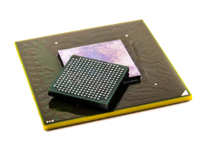
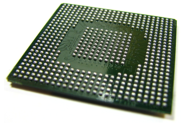
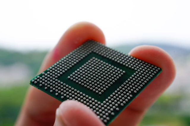
A Ball Grid Array (BGA) is a type of surface-mount packaging in which electrical connections are made through an array of solder balls arranged in a grid pattern on the underside of the package.
These solder balls connect the semiconductor device directly to the PCB pads, forming electrical, mechanical, and thermal connections simultaneously.
Structure of BGA Package
A typical BGA package consists of:
1. Silicon Die
- The core semiconductor chip
- Performs logic, processing, or signal functions
2. Substrate Layer
- Routes signals from die to solder balls
- Made of organic or ceramic materials
- Provides electrical interconnection and mechanical support
3. Solder Balls
- Formed in a precise grid array
- Provide electrical and mechanical connection to PCB
- Common materials: SnAgCu (lead-free solder)
4. Encapsulation
- Protects the die and internal wiring
- Enhances mechanical strength and reliability
Types of BGA Packages
1. Plastic BGA (PBGA)
- Most common type
- Cost-effective
- Used in consumer electronics
2. Ceramic BGA (CBGA)
- High thermal performance
- Used in aerospace and military applications
3. Fine-Pitch BGA (FBGA)
- Smaller ball spacing
- Suitable for compact devices like smartphones
4. Micro BGA (µBGA)
- Ultra-high density
- Used in mobile and wearable devices
5. Flip-Chip BGA (FCBGA)
- Direct die attachment using flip-chip technology
- Excellent electrical performance
- Common in CPUs and GPUs
Advantages of BGA Package
1. High I/O Density
- Supports large number of connections in compact area
- Ideal for complex ICs
2. Improved Electrical Performance
- Shorter interconnect paths
- Reduced inductance and resistance
- Better high-speed signal integrity
3. Better Thermal Performance
- Efficient heat dissipation through solder balls and PCB
- Can be combined with thermal vias
4. Compact Footprint
- Enables smaller PCB designs
- Supports miniaturization of electronics
Challenges of BGA Packaging in PCB Design
Despite its advantages, BGA introduces several manufacturing and design challenges:
1. Routing Complexity
- High pin density requires HDI PCB design
- Often needs via-in-pad and microvia technology
2. Inspection Difficulty
- Solder joints are hidden under the package
- Requires X-ray inspection for quality control
3. Rework Complexity
- Difficult to repair or replace
- Requires specialized rework equipment
4. PCB Manufacturing Precision
- Tight tolerance required for pad alignment
- Strict solder mask and stencil control
PCB Design Considerations for BGA
1. Fan-Out Routing Strategy
- Break out signals using microvias
- Use escape routing techniques
- Optimize layer stack-up for signal distribution
2. Via Design
- Via-in-pad (VIP) for high-density BGAs
- Blind and buried vias for multilayer routing
- Minimize via stub for high-speed signals
3. Signal Integrity
- Maintain controlled impedance routing
- Reduce crosstalk between adjacent signals
- Keep power and ground planes solid
4. Thermal Management
- Use thermal vias under power BGAs
- Connect to internal copper planes
- Improve heat dissipation through PCB stack-up
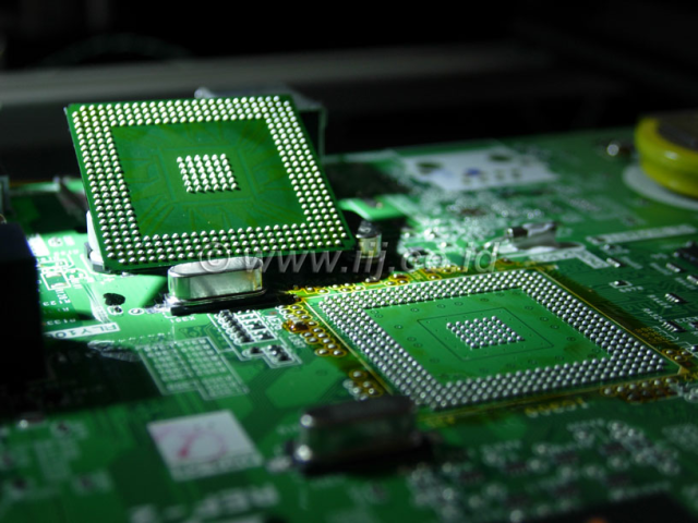
Manufacturing Process of BGA Assembly
1. Solder Paste Printing
- Precise stencil printing required
- Controls solder volume for each ball pad
2. Pick and Place
- High-accuracy placement machines
- Alignment critical due to fine pitch
3. Reflow Soldering
- Controlled thermal profile
- Ensures uniform solder ball melting and bonding
4. Inspection
- Automated Optical Inspection (AOI) for surface components
- X-ray inspection for hidden BGA joints
Applications of BGA Packages
BGA packages are widely used in:
- Microprocessors (CPU, GPU)
- FPGA and ASIC devices
- Networking equipment
- Automotive ECUs
- Industrial control systems
- High-speed communication modules
- AI and computing hardware
Conclusion
The Ball Grid Array (BGA) package is a cornerstone of modern electronics, enabling high-density integration, superior electrical performance, and efficient thermal management. However, it also requires advanced PCB design techniques, precise manufacturing control, and strict quality inspection methods.
As electronic systems continue to demand higher speed and miniaturization, BGA technology will remain a key enabler in high-performance PCB and PCBA solutions.
