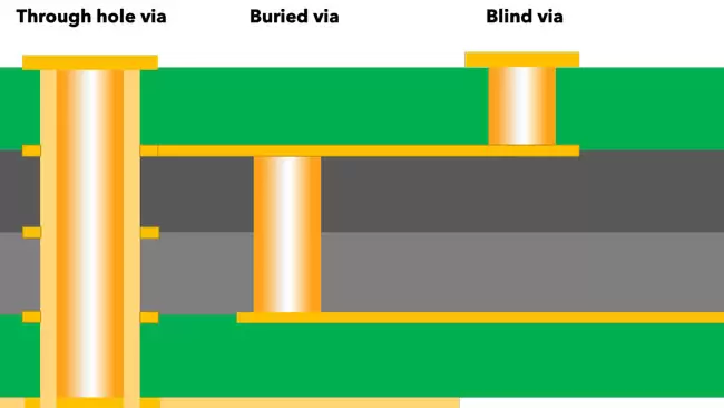
1. Why Buried Via PCB Technology Is Essential for Modern Electronics As modern electronic products continue ev...

1. Why Buried Via PCB Technology Is Essential for Modern Electronics As modern electronic products continue ev...
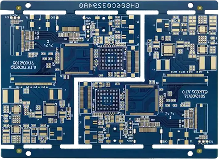
What is a Buried Via PCB? A Buried Via PCB is a multilayer printed circuit board where vias are located betwee...
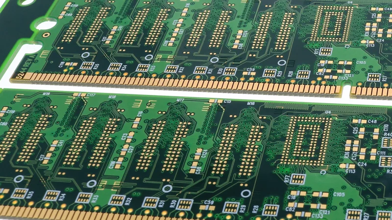
Why Buried Vias Matter As electronic systems become more compact and performance-driven, traditional via struc...
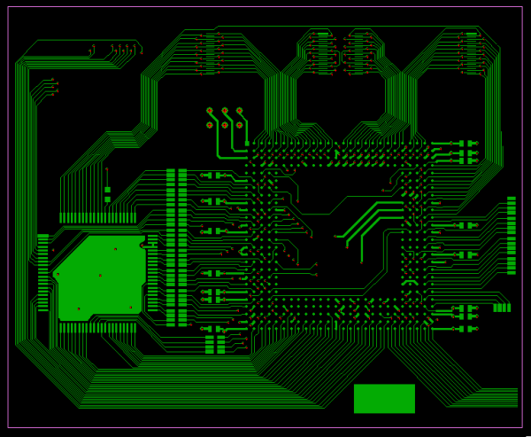
Buried via technology has become essential in modern PCB design, particularly for high-density, high-performan...
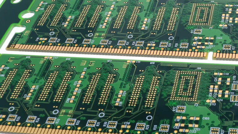
As electronic devices become smaller and more complex, the need for high-density interconnections within print...
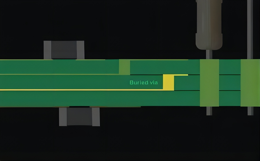
As electronic devices become smaller and more powerful, PCB designers face a constant challenge: fitting more ...
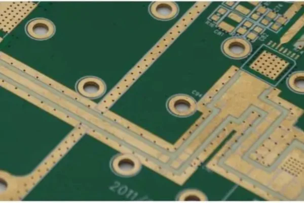
Microvia PCB: High-Density Interconnect Solutions for Advanced Electronics As electronic devices become smalle...
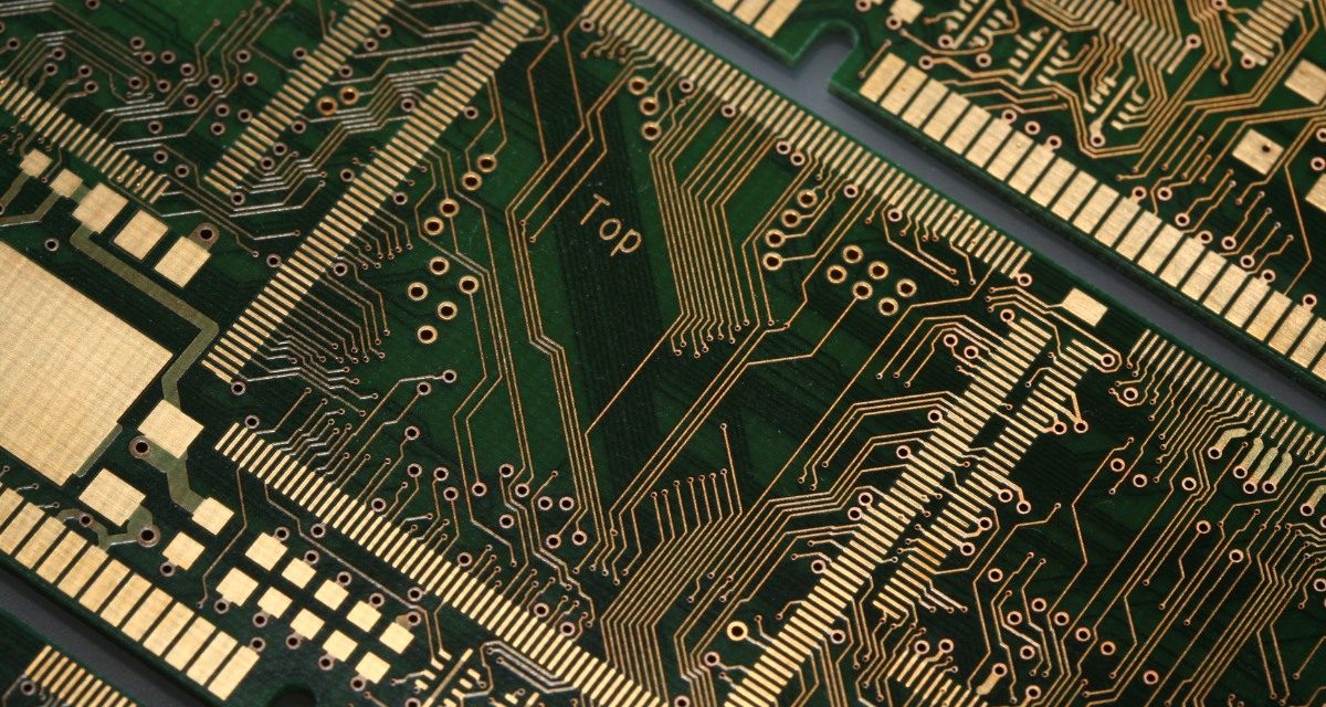
High Density Interconnect (HDI) PCB technology is designed to support modern electronic devices that demand hi...
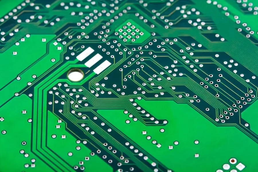
What Is a Buried Via PCB? A Buried Via PCB is a type of multilayer printed circuit board that uses buried vias...
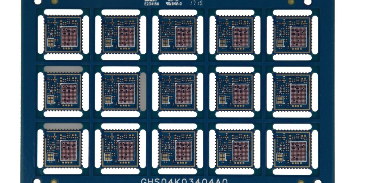
What Is an HDI PCB? An HDI PCB (High Density Interconnect PCB) is a printed circuit board designed with higher...
KKPCBは、フレックス、リジッドフレックス、RF/マイクロ波、HDI、リジッド多層、およびATEテストボード向けのPCB設計、製造、実装、テストを専門とする大手電子ソリューションプロバイダーです。試作、部品調達、SMT/THT実装、機能テスト、筐体組立、最終製品パッケージングを含む包括的なエンドツーエンドサービスを提供しています。ワンストップの社内体制により、KKPCBはOEMおよびODMソリューションを短納期、高品質、コスト効率よく提供し、世界中の顧客にサービスを展開しています。

PCB製造
PCB実装
技術サポート