HomeTag

PTFE PCB - KKPCB

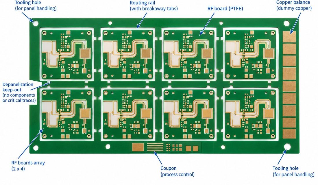
PTFE PCB DFM: Panelization and Procurement Controls for Repeatable RF Builds

A PTFE board can be electrically well designed and still be difficult to quote or panelize. The manufacturing risk is concentrated at the interfaces: copper balance, drilled features, plated edges, hybrid stackup boundaries, connector rails, and the coupon that is supposed to represent the RF path. A PTFE PCB release should therefore explain the process...
PTFE PCB Glass-Weave and Phase Skew: A Routing Review for Wideband Links

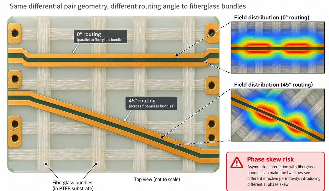
A wideband RF link can show unexplained phase imbalance even when both traces meet the same nominal impedance. On a PTFE PCB, the local resin-to-glass distribution, trace angle, reference-plane spacing, and connector launch can create different effective propagation paths. The project pain is usually discovered after the schematic is stable, when the pair is already...

PTFE PCB Loss Budgets: Copper Profile Checks for Long RF Paths

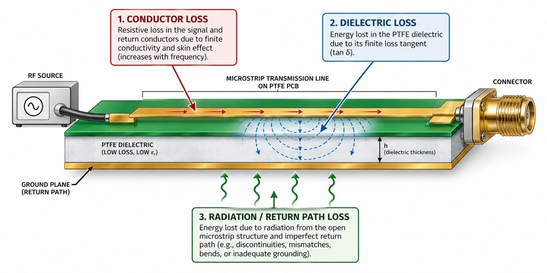
When a microwave path becomes long enough, the material name alone cannot explain insertion loss. A PTFE PCB combines dielectric loss, conductor roughness, trace geometry, resin or ceramic loading, connector transitions, and the return path. Engineers often discover the real problem during a system margin review because the original estimate used a catalog loss tangent...

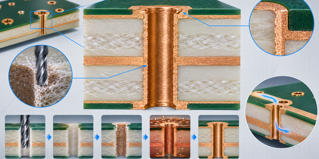
Taconic RF-35 PCB Drill and Plating Control: Avoiding PTFE Via Reliability Escapes

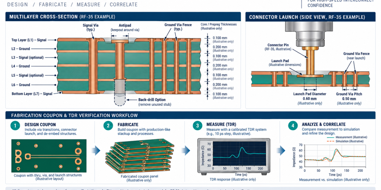
Table of Contents PTFE drilling and stackup RF drill table and transition geometry Desmear and plating controls Coupons and assembly handoff A via can pass an electrical design review and still become the first reliability escape in a PTFE-based RF build. Drill wander on a Taconic RF-35 PCB, smear removal, rough hole walls, poor copper...

Duroid 5880 PCB Stackup: 6 Critical Controls for Stable Impedance Release

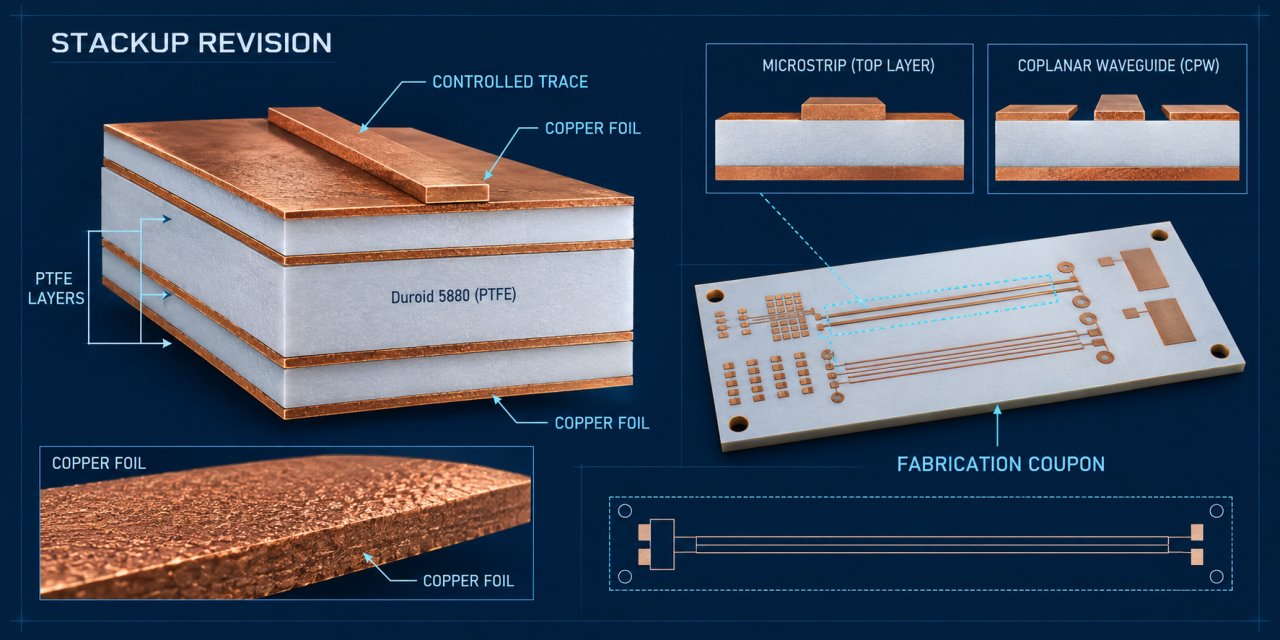
Contents Why stackup drift changes RF behavior Six stackup and impedance controls Coupon and release workflow Release checklist Duroid 5880 PCB stackup decisions determine whether an RF design can move from field model to repeatable fabrication. A nominal dielectric value is not enough. Pressed thickness, copper foil, roughness, trace geometry, and coupon correlation all influence...

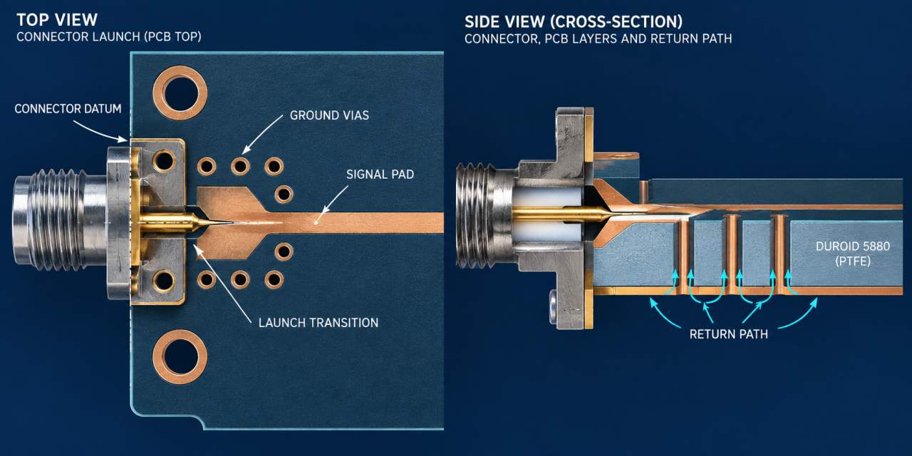
Duroid 5880 PCB Connector Launch: 8 Critical Controls for Repeatable RF Assembly

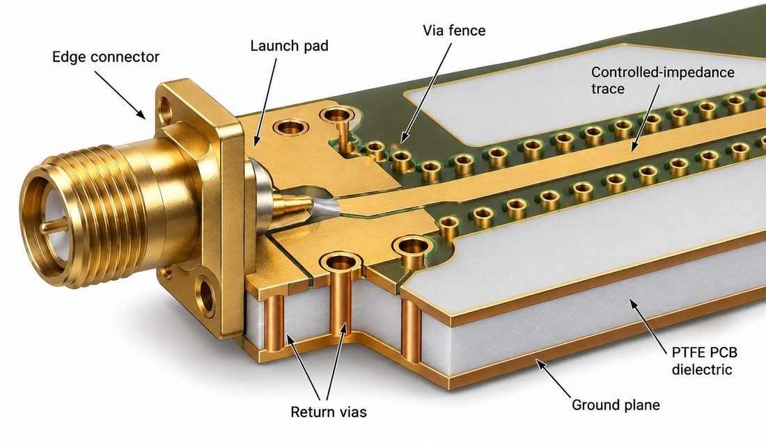
Contents Why the connector launch controls RF yield Layout and datum controls Assembly and inspection controls Release checklist Duroid 5880 PCB connector launches are a common project pain point. A layout can meet the simulated impedance target and still show return-loss variation when the connector datum, plated holes, solder fillet, or ground-via pattern changes during...

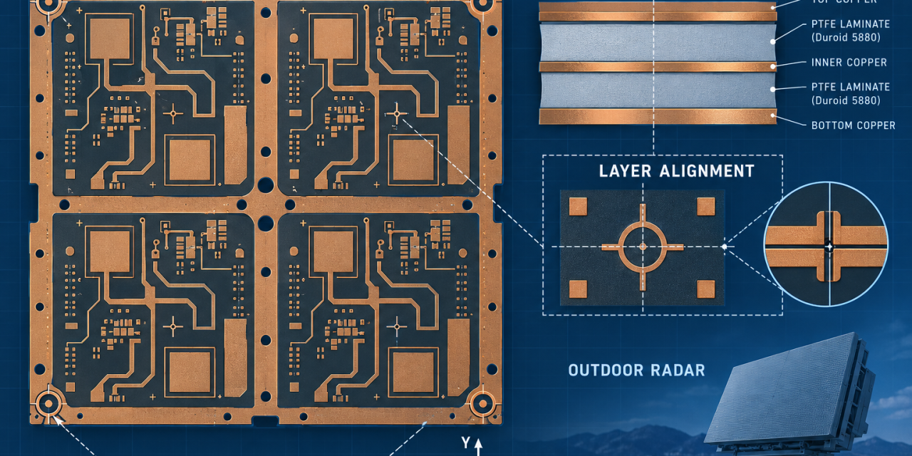
Duroid 5880 PCB Dimensional Stability: 7 Critical Controls

Contents Why dimensional stability becomes an RF problem Seven production controls Outdoor radar release checklist Key takeaway Duroid 5880 PCB projects for outdoor radar often fail at the mechanical-to-RF interface rather than in the laminate specification. Seasonal temperature, moisture conditioning, panel handling, and connector datum changes can move a launch or array cell enough to...