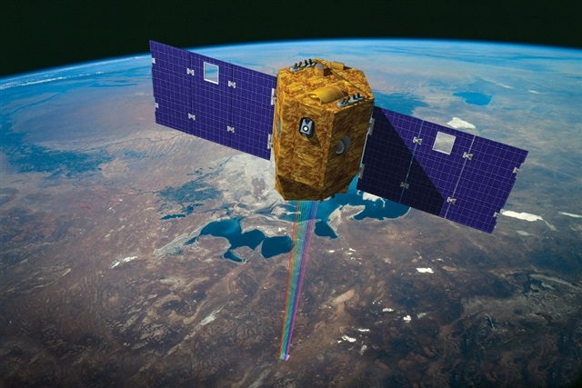
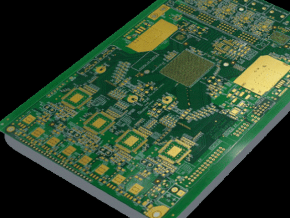
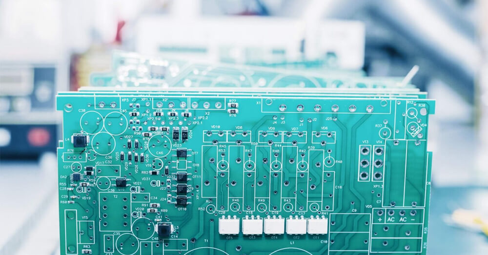
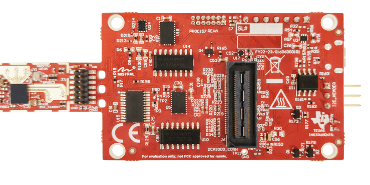
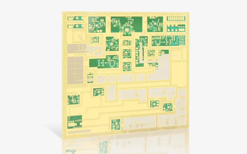
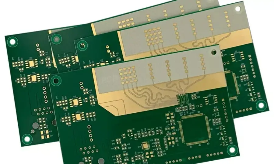
Advanced Engineering Technologies for PCB & PCBA Solutions - KKPCB
 
HomeCategory

Advanced Engineering Technologies for PCB & PCBA Solutions - KKPCB

TLY-5 PCB: High-Frequency Low-Loss PCB Material for RF and Microwave Applications

1.Why TLY-5 PCB Materials Are Important in RF Electronics As RF and microwave systems continue evolving toward: Higher operating frequencies Faster wireless communication Lower signal loss requirements Higher signal integrity standards traditional FR4 PCB materials often cannot meet the electrical performance demands of advanced RF applications. Modern systems such as: 5G communication infrastructure RF power...

RF Transceiver PCB: High-Frequency PCB Design for Wireless Communication Systems

The Importance of RF Transceiver PCB in Wireless Electronics Modern wireless communication systems rely heavily on high-performance RF transceiver circuits to enable: Signal transmission Signal reception Data communication Wireless connectivity As technologies continue advancing toward: 5G and 6G communication IoT devices Automotive radar systems Satellite communication Smart wireless modules the complexity of RF Transceiver PCB...

Satellite PCB: High-Reliability PCB Design for Space and Satellite Communication Systems

1. Introduction: The Role of Satellite PCB in Space Technology Satellite systems operate in one of the most extreme environments in engineering, including: Vacuum conditions Extreme temperature cycling High radiation exposure Long-term mission lifetimes without maintenance Because of these conditions, Satellite PCB design must meet extremely strict reliability, thermal, and electrical performance requirements. Modern satellite...

Low Loss PCB: Materials, Design Principles, and High-Frequency Performance Optimization

1. Introduction: Why Low Loss PCB Is Essential in Modern Electronics As electronic systems evolve toward: Higher data rates Higher operating frequencies Increased signal density Greater system integration traditional PCB materials such as standard FR4 are no longer sufficient for advanced RF and high-speed applications. In modern systems including: 5G/6G communication networks Automotive radar systems...

1. Introduction to Impedance Controlled PCB As modern electronic systems continue advancing toward: Higher frequencies Faster data transmission Higher signal density traditional PCB routing methods are no longer sufficient to guarantee stable signal transmission. In applications such as: 5G communication systems High-speed servers Automotive radar RF and microwave electronics Aerospace communication systems Impedance Controlled PCB...

How to Find FaultyComponents on PCBs: AComprehensive Guide

Troubleshooting printed circuit boards (PCBs) can be a daunting task, but with a systematic approach, it becomes manageable and efficient. This guide provides a step-by-step process to identify faulty components on PCBs, along with methods tailored to specific component types and advanced techniques for batch inspection. Step-by-Step Guide to Finding Faulty Components on PCBs Step 1: Power...

Impedance Controlled PCB: Precision Solutions for High-Speed & RF Signal Integrity

What is an Impedance Controlled PCB? An Impedance Controlled PCB is a printed circuit board designed and manufactured to maintain a specific characteristic impedance for signal traces, ensuring consistent signal transmission. In high-speed and RF designs, the PCB trace behaves like a transmission line. Without proper impedance control, signals can suffer from reflection, distortion, and...

High Tg PCB: High Thermal Stability Solutions for Reliable Electronic Applications

What is a High Tg PCB? A High Tg PCB is a printed circuit board manufactured using materials with a high glass transition temperature (Tg), typically above 170°C. The Tg value represents the temperature at which the PCB material transitions from a rigid state to a softer, more flexible state. A High Tg PCB maintains...

High Layer Count PCB: Advanced Multilayer Solutions for Complex Electronic Systems

What is a High Layer Count PCB? A High Layer Count PCB refers to a multilayer printed circuit board with a large number of layers, typically 10 layers and above, and often reaching 20, 30, or even 50+ layers in advanced applications. A high layer count PCB is designed to handle complex routing, high-speed signals,...

Buried Via PCB: Advanced Multilayer PCB Technology for High-Density Designs

What is a Buried Via PCB? A Buried Via PCB is a multilayer printed circuit board where vias are located between internal layers only, without extending to the outer layers. Unlike through-hole vias, a buried via PCB allows connections between inner layers while keeping the outer layers free for routing, enabling higher circuit density and...