Engineering Technologies – Page 118 – KKPCB
 
HomeCategory

Engineering Technologies

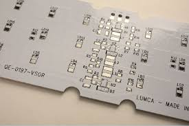
How to Check for PCB Warpage: Techniques and Methods

How to Check for PCB Warpage: Techniques and Methods PCB warpage (also known as bow and twist) is a common manufacturing defect that occurs when a printed circuit board deviates from perfect flatness. It can lead to serious issues during SMT assembly, such as poor solder joint formation, component misalignment, open circuits, or bridging. In...

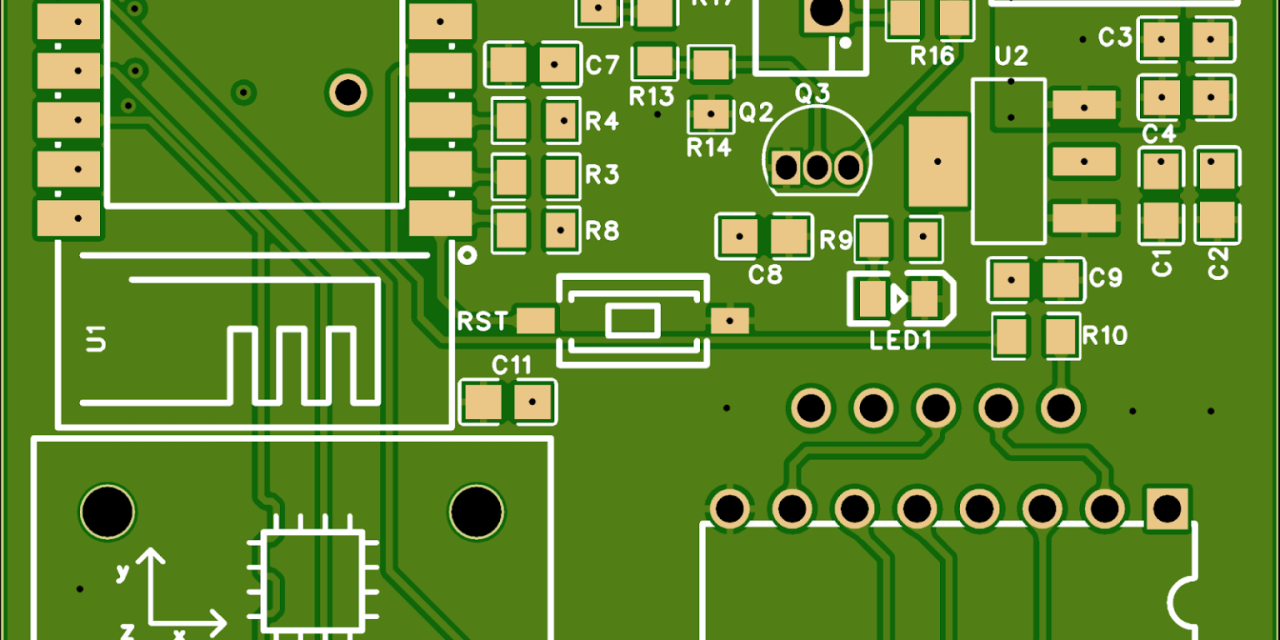
Advanced PCB Footprint Generator: Key to Efficient PCB Design

1. Introduction: Why PCB Footprint Accuracy Matters in Modern Electronics In modern PCB design and electronic product development, accuracy at the earliest design stage directly determines manufacturing success, cost efficiency, and product reliability. One of the most critical elements in PCB layout design is the PCB footprint, which defines the physical land pattern for electronic...

How to Find Faulty Components on PCBs: A Comprehensive Guide

Troubleshooting printed circuit boards (PCBs) can be a daunting task, but with a systematic approach, it becomes manageable and efficient. This guide provides a step-by-step process to identify faulty components on PCBs, along with methods tailored to specific component types and advanced techniques for batch inspection. Step-by-Step Guide to Finding Faulty Components on PCBs Step 1: Power...

Exploring the Current Carrying Capacity of Flexible PCBs

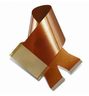
Flexible PCBs, commonly made from polyimide materials, are known for their amber color and ability to withstand high temperatures, often comparable to or exceeding those of FR4 boards. The current carrying capacity of flexible PCBs is primarily determined by factors such as copper thickness, trace width, and material properties. With a relative tracking index (CTI) typically above 600 volts, these PCBs are suitable for...

Optimizing PCB Trace Thickness vs. Current Capacity

The relationship between PCB trace thickness and current capacity is a critical aspect of PCB design. Properly sizing traces ensures that they can handle the required current without overheating, which is essential for the reliability and functionality of the circuit. This article explores the key considerations for selecting trace thickness, the impact of copper weight, and...

PCB Routing: Best Practices for Ensuring Signal Integrity and Performance

Printed Circuit Board (PCB) routing is a critical aspect of electronic design, ensuring that electrical signals are transmitted efficiently and reliably between components. Proper routing minimizes interference, maintains signal integrity, and meets design requirements such as impedance control and thermal management. This article outlines the best practices for PCB routing, focusing on optimizing performance and ensuring signal integrity....

Sensors and Transducers in Your PCB Design

Sensors and transducers play integral roles in PCBs by enabling electronic systems to interact with and respond to the surrounding environment. Sensors detect physical parameters such as temperature, pressure, light, and motion, converting these analog signals into electrical signals that PCBs process. Sensors are used in various applications, from environmental monitoring and industrial automation to consumer electronics. By integrating...

Materials for High Temperature PCBs

Introduction: Why High Temperature PCB Materials Matter In demanding electronic applications, high temperature PCBs are essential for ensuring stable performance, long-term reliability, and safe operation under extreme thermal conditions. Industries such as automotive electronics, aerospace systems, power electronics, and industrial automation require PCB materials that can withstand elevated temperatures without degradation. Choosing the right materials...

The Most Common Manual PCB Soldering Defects

Why Manual PCB Soldering Quality Matters Although automated SMT PCB assembly is widely used in modern electronics manufacturing, manual PCB soldering remains essential for: Prototype PCB assembly Through-hole PCB assembly (THT) PCB rework and repair Low-volume electronics manufacturing Industrial and aerospace electronics maintenance However, improper manual soldering techniques can easily create PCB soldering defects, affecting:...

Ball Grid Array Technology Overview

What Is Ball Grid Array (BGA) Technology? Ball Grid Array (BGA) is an advanced surface mount packaging technology widely used in modern electronic products requiring high pin counts, high-speed signal transmission, and compact PCB layouts. Unlike traditional leaded packages, BGA components use an array of solder balls located underneath the package to create electrical and...