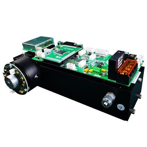
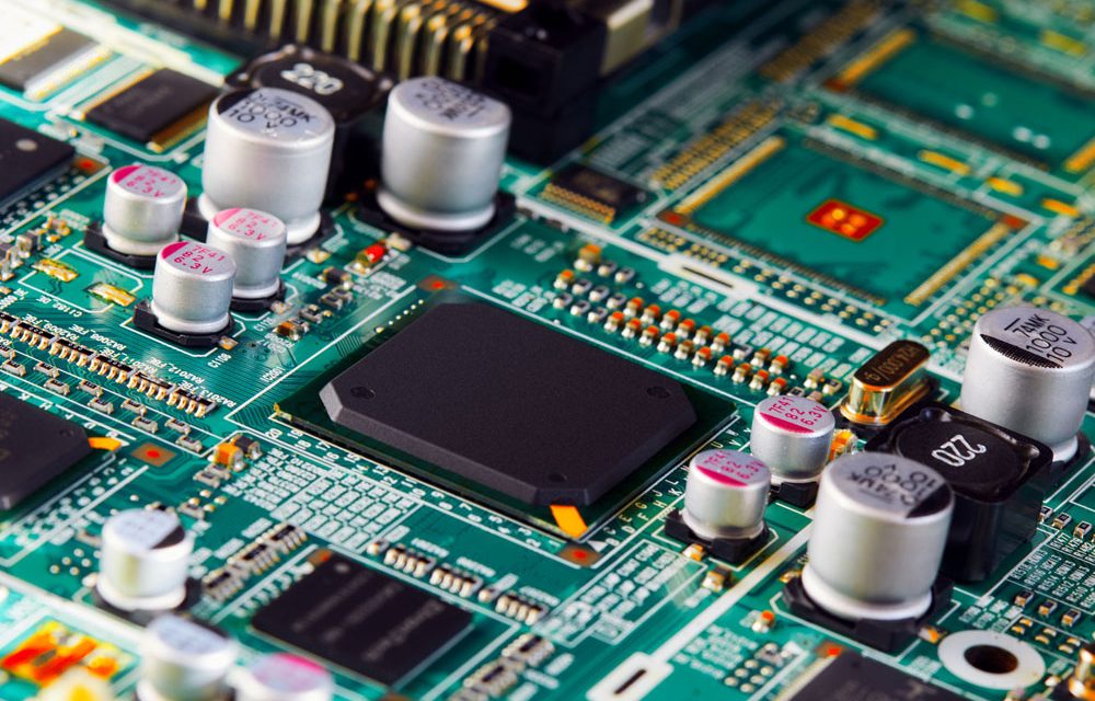
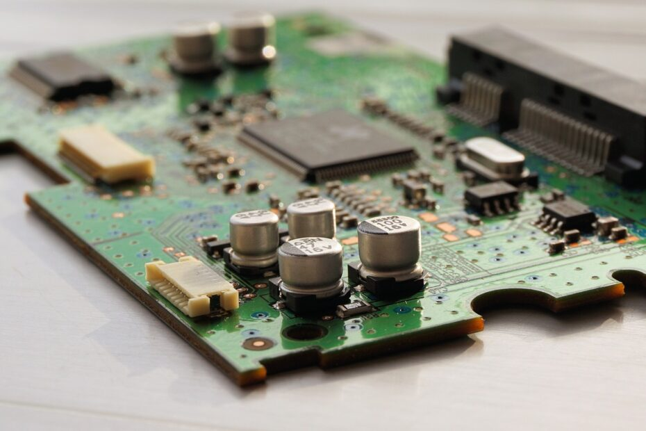
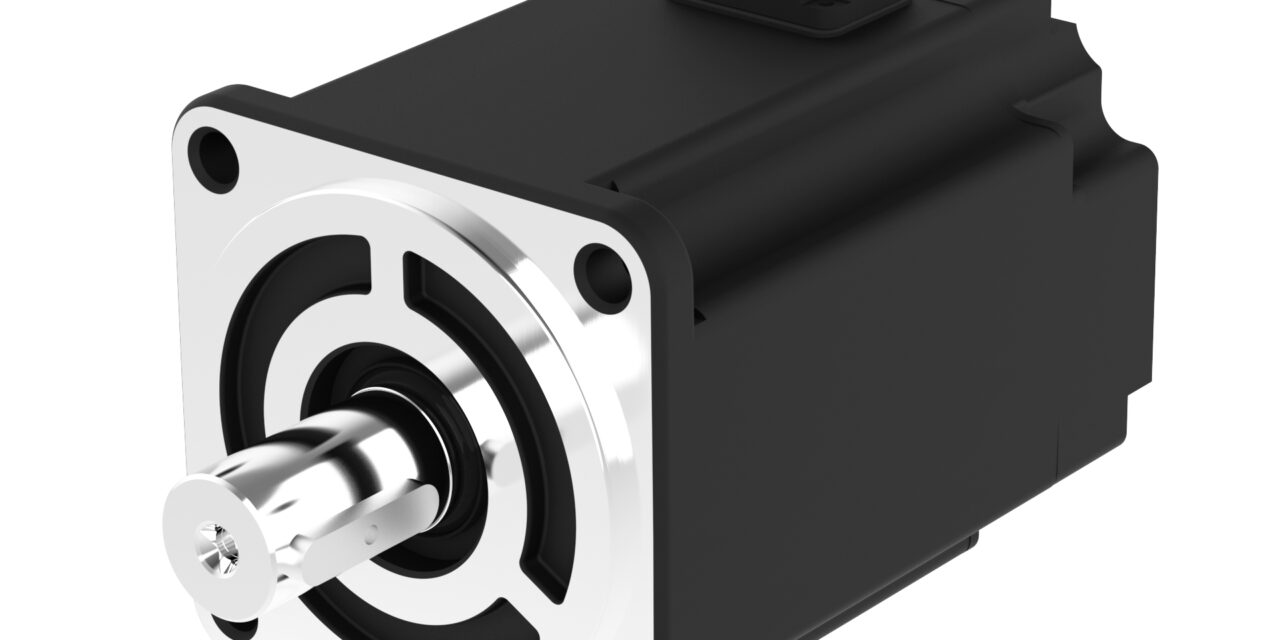
KKPCB Blog – PCB & PCBA Insights, News, and Tips - KKPCB
 

Blog

Explore the KKPCB Blog for the latest PCB manufacturing and assembly news, industry insights, expert tips, and technology trends, helping you stay informed and optimize your electronics projects.
What is the difference between immersion gold and gold plating in PCB?

Surface finishes in PCBs are vital for ensuring solderability, electrical conductivity, and corrosion resistance. They help components bond securely to the board, ensure smooth signal flow, and protect the PCB from environmental damage. Without a proper surface finish, a PCB may not function correctly or could wear out faster. Immersion Gold (ENIG) and Gold Plating are two popular gold...

As we step into 2025, the electronics manufacturing industry is poised for transformative changes driven by technological advancements, shifting consumer demands, and global economic factors. At KKPCB, we are committed to staying at the forefront of these developments to deliver cutting-edge solutions to our clients. Here’s an overview of the key trends set to reshape the...

To develop and realize Hybrid PCBs for space applications through indigenous vendors

A Hybrid Printed Circuit Board (PCB) is a multilayer PCB that combines dissimilar materials to optimize electrical performance, improve system reliability, and enhance high-frequency RF applications. These PCBs utilize materials with significantly different critical properties compared to traditional multilayer PCBs. Hybrid PCBs may incorporate a mix of FR-4 materials with high-frequency PTFE materials, or use a combination of various...

Standard PCB Thickness and Optimization

When designing a printed circuit board (PCB), engineers often focus on ensuring the correct impedance structures and electrical performance of the board. However, the physical characteristics, such as PCB thickness, are equally important and can significantly impact the cost, manufacturability, and performance of the final product. While standard PCB thicknesses are widely used, they are more of a...

PCB Design For Military & Aerospace Applications

Military and aerospace PCBs must adhere to intensely high standards to ensure their safety and functionality in the extreme conditions they’re used in. For this reason, PCB design for military and aerospace applications requires incredibly stringent guidelines with built in redundancy, extra safety, and stringent tolerances, minimizing risk of failure. General PCB Design Tips for Military and Aerospace Applications...

Low Power Circuit Design Strategies for PCBs

Low power circuit design includes strategies focused on minimizing both dynamic and static power usage in your printed circuit boards. While selecting components with low power requirements is a crucial element, low power PCB design involves more comprehensive considerations to effectively manage power consumption. Lower Power Circuit Designs Tips Aspect Description Identify Major Power Consumers Start by...

RF Via Transitions in High-Speed Designs: Best Practices and Considerations

In high-speed and RF PCB designs, controlling trace impedance is critical, but the role of RF via transitions is often underestimated. Vias, which connect signals between layers, can introduce impedance mismatches, signal reflections, and losses, especially at high frequencies. Proper design and optimization of via transitions are essential to maintain signal integrity and ensure reliable performance in RF and...

How to Check for PCB Warpage: Techniques and Methods

How to Check for PCB Warpage: Techniques and Methods PCB warpage (also known as bow and twist) is a common manufacturing defect that occurs when a printed circuit board deviates from perfect flatness. It can lead to serious issues during SMT assembly, such as poor solder joint formation, component misalignment, open circuits, or bridging. In...

Advanced PCB Footprint Generator: Key to Efficient PCB Design

1. Introduction: Why PCB Footprint Accuracy Matters in Modern Electronics In modern PCB design and electronic product development, accuracy at the earliest design stage directly determines manufacturing success, cost efficiency, and product reliability. One of the most critical elements in PCB layout design is the PCB footprint, which defines the physical land pattern for electronic...