
With the increasing demand for smart homes, low-carbon electronics, and maintenance-free IoT devices, battery-free wireless doorbells are becoming an innovative solution for next-generation home automation systems.
Traditional wireless doorbells typically rely on batteries to power the transmitter module. However, battery-powered designs may face challenges such as:
- Limited battery lifespan
- Regular battery replacement requirements
- Increased maintenance costs
- Environmental concerns caused by battery disposal
A battery-free wireless doorbell adopts energy harvesting technology to capture mechanical energy generated when a user presses the button and convert it into electrical energy to transmit wireless signals.
In this application, the PCBA (Printed Circuit Board Assembly) plays a critical role in integrating:
- Energy harvesting circuits
- Power management circuits
- Wireless communication modules
- Control ICs
- Signal processing functions
This case study introduces how KKPCB supported the development of an energy harvesting PCBA solution, helping improve product reliability, miniaturization, and manufacturing readiness.
1. Project Background
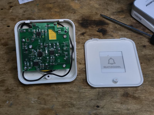
A customer developing a battery-free wireless doorbell system required a compact and reliable PCBA solution for smart home applications.
Unlike conventional wireless doorbells, the product needed to operate without an external power source. When a user presses the mechanical button, the internal energy harvesting mechanism generates a small amount of electrical energy, which powers the wireless transmitter.
The product requirements included:
- Battery-free operation
- Compact PCB size
- Low-power circuit design
- Stable wireless signal transmission
- High production consistency
During prototype-to-production transition, the customer faced several PCB-level challenges related to energy conversion efficiency, circuit integration, and manufacturing reliability.
2. Key Challenges in Battery-Free Doorbell PCBA Development
Challenge 1: Efficient Energy Harvesting Circuit Integration
Customer Pain Point
The available energy generated from mechanical pressing was limited.
The PCBA needed to efficiently manage and utilize a small amount of harvested energy to support:
- Power conversion
- Signal processing
- Wireless transmission
Potential issues included:
- Energy loss during conversion
- Insufficient power stability
- Unstable wireless triggering
The circuit design required careful optimization of:
- Power paths
- Component selection
- Energy storage management
Challenge 2: Low-Power Circuit Design
Customer Pain Point
Since the system does not use batteries, every part of the circuit must operate with extremely low power consumption.
Challenges included:
- Minimizing standby power consumption
- Ensuring sufficient energy for transmission
- Reducing unnecessary circuit losses
The PCBA required optimized:
- Power management circuits
- MCU operation modes
- Wireless communication timing
Challenge 3: Compact PCB Design and Component Integration
Customer Pain Point
The doorbell transmitter module had limited internal space.
The PCB needed to integrate:
- Energy harvesting circuit
- Power management module
- Wireless communication circuit
- Control components
within a small form factor.
Design challenges included:
- Component placement
- Signal routing
- Noise control
- Manufacturing accessibility
Challenge 4: Wireless Signal Reliability
Customer Pain Point
The doorbell required stable wireless communication after energy generation.
Potential risks included:
- Insufficient transmission power
- Signal interference
- Poor antenna layout
PCB design needed to consider:
- RF signal path
- Grounding structure
- EMI control
- Antenna placement
Challenge 5: Transition from Prototype to Mass Production
Customer Pain Point
The prototype demonstrated basic functionality, but production required improvements in:
- Assembly consistency
- Manufacturing yield
- Testing efficiency
Potential risks included:
- Small component assembly difficulties
- Soldering reliability
- Functional test limitations
3. KKPCB Engineering Support and Solutions
3.1 PCB Design Review and DFM Optimization
Before production, KKPCB engineering team performed a detailed review of:
- PCB layout
- Component placement
- Manufacturing feasibility
- Assembly requirements
Optimization focused on:
- Improving component accessibility
- Reducing assembly risks
- Enhancing production consistency
- Preparing functional testing points
This helped create a smoother transition from prototype validation to production.
3.2 Power Management Optimization
To improve energy utilization efficiency, the PCBA design was optimized for:
Energy Conversion Path
The engineering team focused on:
- Minimizing power losses
- Optimizing component selection
- Improving power transfer efficiency
Power Distribution Design
The PCB layout was optimized to ensure:
- Shorter power paths
- Reduced resistance losses
- Improved circuit stability
3.3 Low-Power Circuit Optimization
The PCBA design was optimized through:
- Efficient component selection
- Reduced unnecessary power consumption
- Improved control timing
The solution helped ensure that limited harvested energy could effectively support:
- Signal processing
- Wireless transmission
- System triggering
3.4 RF and Signal Integrity Improvement
For wireless communication reliability, PCB optimization included:
- Improved RF routing
- Better grounding design
- Reduced interference sources
- Optimized antenna connection area
These improvements enhanced:
- Wireless transmission stability
- Signal consistency
- Product reliability
3.5 Manufacturing Process Optimization
To support production requirements, KKPCB provided:
- SMT assembly support
- Process optimization
- Inspection solutions
Quality control included:
- SPI solder paste inspection
- AOI inspection
- Functional testing
This ensured stable assembly quality and production repeatability.
4. Manufacturing and Quality Control Process
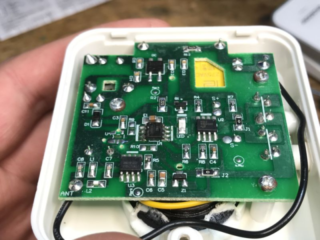
PCB Fabrication
The battery-free doorbell PCBA required careful control of:
- PCB thickness
- Copper distribution
- Surface finish
- Dimensional accuracy
Material selection considered:
- Electrical performance
- Mechanical reliability
- Production requirements
SMT Assembly
The assembly process included:
Solder Paste Printing
Controlled solder paste volume ensured reliable connections for fine-pitch components.
Automated Placement
High-precision placement equipment assembled:
- IC components
- Passive devices
- Wireless modules
Reflow Soldering
Optimized thermal profiles ensured:
- Stable solder joints
- Reduced thermal stress
Inspection and Testing
Quality verification included:
AOI Inspection
Checking:
- Component placement
- Solder quality
- Assembly defects
Functional Testing
Validation included:
- Energy harvesting response
- Wireless transmission
- Trigger reliability
5. Project Results
Through PCB design optimization, energy management improvement, and manufacturing process control, the project achieved:
- Successful battery-free operation
- Improved energy utilization efficiency
- Enhanced wireless communication stability
- Improved production consistency
Production validation results included:
- 98%+ first-pass production yield
- Reduced prototype-to-production transition risks
- Improved product reliability during long-term operation
6. Key Engineering Insights
6.1 Energy Harvesting Products Require System-Level Optimization
For battery-free devices, PCB design is not only about circuit connection.
It must consider:
- Energy availability
- Power conversion efficiency
- Component consumption
- Communication requirements
6.2 Low-Power Design Is Critical for Self-Powered Devices
When available energy is limited, every circuit block affects system performance.
Optimized design requires:
- Efficient power architecture
- Low-power components
- Reduced energy loss
6.3 RF Reliability Depends on PCB-Level Design
Wireless products require careful consideration of:
- Antenna layout
- Grounding
- Signal routing
- EMI control
A well-designed PCB helps ensure stable wireless communication.
7. Applications of Similar Energy Harvesting PCBA Solutions
Energy harvesting PCBAs can support applications including:
Smart Home Devices
- Battery-free switches
- Wireless controllers
- Smart sensors
Industrial IoT Devices
- Wireless monitoring nodes
- Self-powered sensors
- Equipment status indicators
Building Automation Systems
- Smart access control
- Wireless control panels
- Energy-saving devices
Wearable and Portable Electronics
- Low-power sensing devices
- Self-powered monitoring systems
Conclusion
The development of a battery-free wireless doorbell requires advanced PCBA design capabilities that combine:
- Energy harvesting technology
- Low-power circuit design
- RF communication optimization
- Compact PCB integration
- Manufacturing reliability
In this project, KKPCB supported the customer through PCB design optimization, power management improvement, RF reliability enhancement, and production process control, helping transform an innovative energy harvesting concept into a stable and manufacturable electronic product.
As smart home and IoT technologies continue evolving, customized PCBA solutions will play an increasingly important role in enabling maintenance-free, energy-efficient, and intelligent electronic devices.





