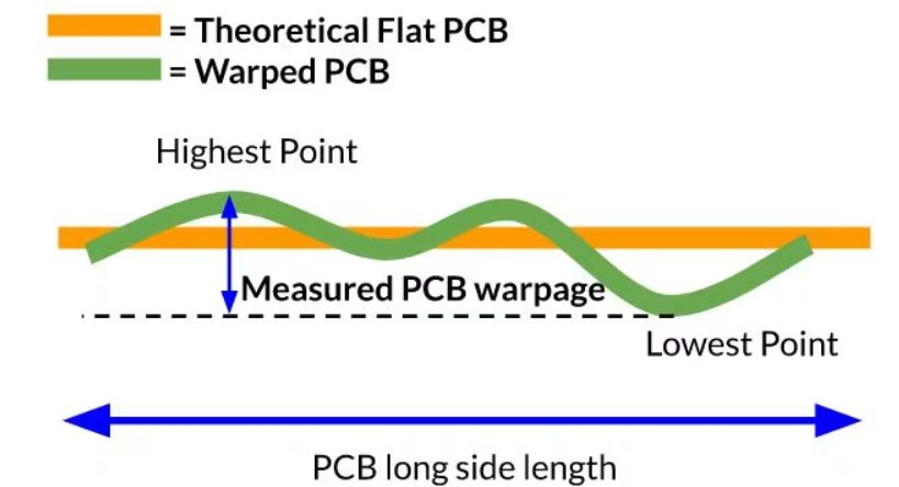
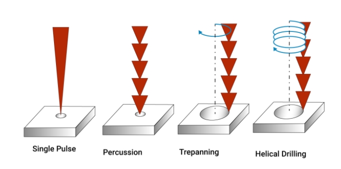
KKPCB Blog – PCB & PCBA Insights, News, and Tips - KKPCB
 

Blog

Explore the KKPCB Blog for the latest PCB manufacturing and assembly news, industry insights, expert tips, and technology trends, helping you stay informed and optimize your electronics projects.
Comprehensive Guide: From PCB to MCU — Effective Anti-Interference Design

Printed Circuit Boards (PCBs) play a crucial role in supporting and connecting electronic components, while interference can significantly impact their performance. This guide explores anti-interference design principles for PCBs and microcontrollers (MCUs) to ensure reliable operation in high-noise environments. Key Principles of PCB Anti-Interference Design 1. Ground Wire Layout Separate Digital and Analog Ground: Isolate digital and...

Pros and Cons of Copper Coating in PCB Design

Copper coating, also known as copper filling, is an essential aspect of PCB design that plays a key role in reducing impedance, improving anti-interference capabilities, and enhancing the overall efficiency of power delivery. However, there are several factors to consider when applying copper coating, and the effectiveness depends on how well it is executed. Let’s explore the...

Detailed Explanation of PCB Manufacturing Process and Precautions

High-quality PCB production begins with high-quality design. Huaqiang PCB manufacturing heavily relies on the cooperation of the design process. Engineers, please design your PCBs according to the detailed explanation of the conventional production process below. Design Parameters for PCB Manufacturing 1. Via (Conductive Hole) Minimum hole diameter: 0.3mm (12mil) The minimum via hole diameter is 0.3mm, and...

Mobile Phone PCB Layout: Key Considerations and Wiring Best Practices

PCB layout in mobile phone design requires meticulous attention to minimize risks and ensure optimal performance. With multiple layers dedicated to various functions, specific guidelines help maintain signal integrity and reduce electromagnetic interference (EMI). Below are the detailed issues and wiring principles to consider in mobile phone PCB layout, especially for complex components like RF circuits...

How to Deal with Power Supply Noise Interference in PCB Design

Power supply noise interference is a critical challenge in PCB design, particularly in high-frequency circuits. Noise from the power supply can significantly impact signal integrity and overall circuit performance. This article provides an in-depth analysis of power supply noise, its causes, and practical strategies to mitigate interference in PCB design. Understanding Power Supply Noise Power supply...

Basic Rules for PCB Layout and Wiring

I. Component Layout Rules Module-Based Layout: Group related components that serve the same function into a module. Separate digital and analog circuits to minimize interference. Clearance Around Holes: Non-mounting holes (e.g., positioning holes): Keep a 1.27mm clearance around them. Mounting holes (e.g., screw holes): Maintain 3.5mm clearance for M2.5 screws and 4mm for M3 screws. Avoid Vias Under Components: Do not place vias under horizontal...

PCB Material Selection Guide

Selecting the right PCB material is not just a design choice—it directly impacts signal integrity, thermal performance, manufacturability, and long-term reliability. For engineers and sourcing professionals, material selection often becomes the hidden factor behind project success or failure, especially in high-frequency, high-speed, or harsh-environment applications. This guide breaks down how to choose PCB materials based...

How Are Printed Circuit Boards Manufactured?

Circuit boards play a key role in making sure electronic products work properly. They provide structural support and link all the electrical parts together. Whether it’s in smartphones, laptops, or household devices, none could operate without a PCB. This guide will introduce you to the components of a printed circuit board and help you understand the manufacturing process....