
Space electronic systems require printed circuit boards (PCBs) with exceptional levels of reliability, environmental resistance, and long-term operational stability. Unlike conventional commercial electronics, space applications must withstand extreme conditions including:
- Large temperature variations
- Mechanical vibration and shock
- Radiation exposure
- Vacuum environments
- Long mission durations without maintenance
As spacecraft systems become more sophisticated, PCB technology must continue evolving to support:
- High-density electronic integration
- High-speed signal transmission
- Power management
- Miniaturized system designs
Among advanced PCB technologies, Hybrid PCBs have gained increasing attention due to their ability to combine different substrate materials and electrical characteristics within a single circuit structure.
Developing hybrid PCBs through qualified domestic manufacturing capabilities helps improve supply chain independence, reduce external dependency, and strengthen local manufacturing ecosystems for advanced electronic systems.
1. What Are Hybrid PCBs?
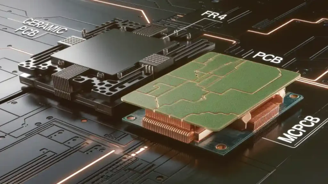
A Hybrid PCB is a circuit board structure that combines different PCB materials or technologies within one design to achieve optimized electrical, thermal, mechanical, or reliability performance.
Unlike conventional PCBs manufactured from a single substrate material, hybrid PCBs may integrate:
- Standard FR-4 materials
- High-frequency laminates
- Ceramic substrates
- Metal-core materials
- Low-loss dielectric materials
The purpose is to combine the advantages of different materials while balancing:
- Cost
- Performance
- Manufacturability
- Reliability
2. Why Hybrid PCBs Are Important for Space Applications
Space electronics require PCBs that can operate reliably under demanding environmental conditions.
Hybrid PCB technology provides several advantages.
2.1 High Reliability Under Extreme Environments
Space systems may experience:
- Extreme temperature cycling
- Vacuum conditions
- Radiation exposure
- Long operational periods
Hybrid PCB structures can be optimized by selecting materials with suitable:
- Thermal expansion characteristics
- Mechanical strength
- Electrical stability
2.2 Improved Thermal Management
Space electronics often operate with limited cooling options.
Hybrid PCB structures can combine materials with better thermal performance, such as:
- Ceramic substrates
- Metal-based materials
Benefits include:
- Improved heat dissipation
- Reduced thermal stress
- Better component reliability
2.3 Enhanced High-Frequency Performance
Modern spacecraft increasingly rely on:
- Communication systems
- Radar systems
- Navigation electronics
These applications require stable RF performance.
Hybrid PCB designs can integrate low-loss materials to achieve:
- Lower signal attenuation
- Better impedance stability
- Improved phase consistency
3. Key Challenges in Hybrid PCB Development
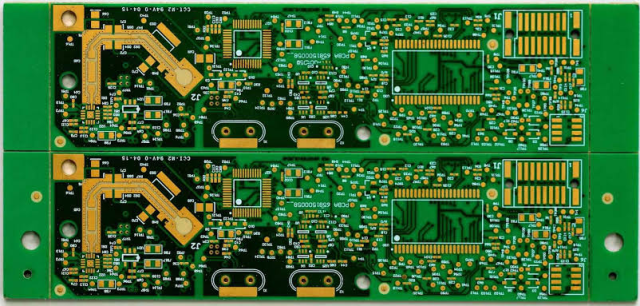
3.1 Material Compatibility
Combining different materials introduces challenges related to:
- Coefficient of thermal expansion (CTE)
- Moisture absorption
- Mechanical stress
Poor material compatibility may result in:
- Layer separation
- Cracking
- Reliability degradation
Therefore, material selection and lamination process control are critical.
3.2 Complex Manufacturing Processes
Hybrid PCB manufacturing requires precise control of:
- Material bonding
- Layer alignment
- Drilling processes
- Copper plating
Compared with standard PCBs, hybrid structures require:
- More advanced manufacturing capability
- More detailed process verification
3.3 High Reliability Requirements
Space applications require strict quality control.
Important considerations include:
- Via reliability
- Solder joint reliability
- Material stability
- Electrical performance consistency
Manufacturers need comprehensive inspection and testing procedures.
4. Manufacturing Process of Hybrid PCBs
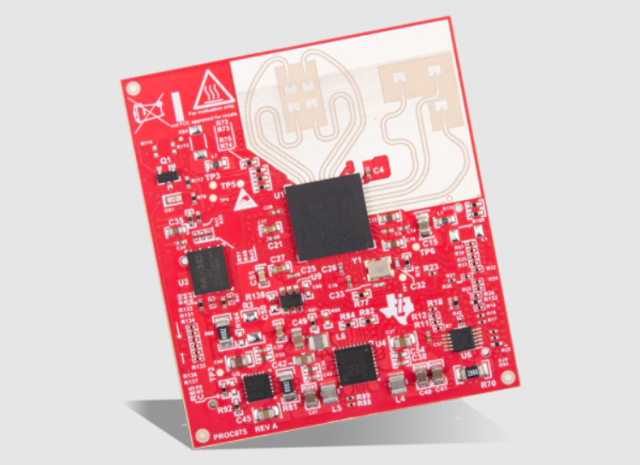
4.1 Engineering Design and Material Evaluation
Before manufacturing, engineers evaluate:
- Electrical requirements
- Thermal conditions
- Mechanical constraints
- Mission environment
Key design considerations include:
- Stack-up structure
- Material compatibility
- Impedance requirements
4.2 Material Preparation
Selected materials are prepared according to design requirements.
Possible combinations include:
- FR-4 + ceramic
- FR-4 + high-frequency laminate
- Low-loss material + thermal substrate
Material preparation requires strict control of:
- Thickness
- Surface treatment
- Cleanliness
4.3 Layer Lamination
The lamination process combines different materials into a unified PCB structure.
Critical parameters include:
- Temperature
- Pressure
- Lamination cycle
Poor process control may lead to:
- Delamination
- Internal stress
- Structural instability
4.4 Precision Drilling and Plating
Hybrid PCBs often require advanced drilling processes:
- Mechanical drilling
- Laser drilling
- Controlled-depth drilling
Copper plating quality directly affects:
- Electrical connectivity
- Mechanical reliability
4.5 Inspection and Reliability Testing
Space-grade PCBs require strict verification, including:
Electrical Testing
Used to verify:
- Continuity
- Insulation resistance
- Signal performance
X-Ray Inspection
Used for:
- Internal defects
- Layer connection quality
Thermal Testing
Evaluates:
- Temperature cycling performance
- Material stability
Mechanical Testing
Includes:
- Vibration testing
- Shock testing
5. Advantages of Developing Hybrid PCBs Through Indigenous Vendors
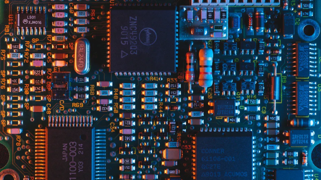
Developing hybrid PCB capabilities through domestic suppliers provides several strategic benefits.
5.1 Improved Supply Chain Control
Local manufacturing capability helps:
- Reduce dependence on overseas suppliers
- Improve supply stability
- Shorten communication cycles
5.2 Faster Engineering Collaboration
Close cooperation between:
- PCB designers
- Material suppliers
- Manufacturing engineers
helps accelerate:
- Prototype development
- Design optimization
- Production improvements
5.3 Development of Advanced Manufacturing Capability
Building local expertise in hybrid PCB production supports:
- Advanced PCB technologies
- High-reliability electronics
- Future space missions
6. Applications of Hybrid PCBs in Space Electronics
Hybrid PCB technology can support various space-related electronic systems.
Satellite Communication Systems
Requirements:
- High-frequency performance
- Low signal loss
- Long-term stability
Navigation and Control Electronics
Requirements:
- High reliability
- Precise signal processing
- Environmental resistance
Power Management Systems
Requirements:
- Thermal performance
- High current capability
- Electrical reliability
Payload Electronics
Requirements:
- Compact integration
- Stable operation
- Radiation tolerance
7. Future Development Trends of Space Hybrid PCB Technology
Higher Integration Density
Future space electronics will require:
- Smaller PCB structures
- Higher layer counts
- Advanced interconnection technologies
Advanced Material Development
Future hybrid PCBs may integrate:
- Advanced ceramics
- Low-loss materials
- Thermal management substrates
Improved Domestic Manufacturing Capability
The development of indigenous hybrid PCB manufacturing will focus on:
- Process optimization
- Reliability improvement
- Automated inspection
Conclusion
Hybrid PCBs provide an effective solution for space electronic systems requiring high reliability, advanced electrical performance, and environmental durability.
Developing and manufacturing hybrid PCBs through qualified indigenous vendors requires comprehensive control over:
As space electronics continue evolving toward higher performance and greater integration, hybrid PCB technology will play an increasingly important role in enabling reliable next-generation aerospace systems.
