Blog

Explore the KKPCB Blog for the latest PCB manufacturing and assembly news, industry insights, expert tips, and technology trends, helping you stay informed and optimize your electronics projects.
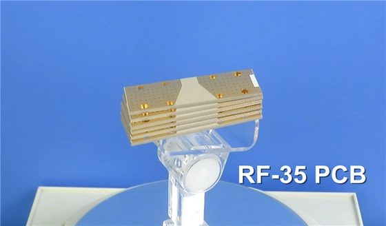
RO4830™ Material: Driving the Popularization of Millimeter-Wave Radar in Automotive Active Safety Systems

RO4830™ is a hydrocarbon resin-based high-frequency laminate designed for 77 GHz automotive radar, 60 GHz traffic radar, and industrial applications. Low-loss, reliable, and cost-effective, it ensures excellent electrical performance, thermal stability, and precise manufacturability for high-frequency PCB designs.

The Critical Issue of Near Holes in Multi-Layer PCB Design

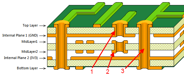
In multi-layer PCB design, the primary focus during routing is to ensure efficient and reliable electrical connections between layers using vias. However, as PCB density increases, vias often need to be placed closer together, leading to design and manufacturing challenges. These challenges not only complicate the production process but also impact the long-term reliability of the product....

Experience Sharing in Multi-Layer PCB Impedance Line Routing

With the continuous development of high-speed electronic systems, PCB design is facing increasingly demanding requirements for signal transmission performance. In applications such as communication equipment, industrial control systems, automotive electronics, semiconductor testing equipment, and RF systems, maintaining stable signal quality has become a key factor affecting product reliability. In multilayer PCB design, impedance-controlled routing is...

High-Speed PCB: Optimal Six-Layer Board Structure

When designing high-speed PCBs, the layer stack-up plays a crucial role in ensuring signal integrity, minimizing crosstalk, and achieving optimal electromagnetic compatibility (EMC). For a standard six-layer board with a thickness of 1.6mm, selecting the right structure can significantly impact performance. Below is an analysis of common six-layer board structures and their suitability for high-speed designs....

Basic Knowledge You Need to Master for PCB Design

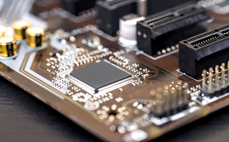
PCB (Printed Circuit Board) design is a fundamental process in electronic product development. A well-designed PCB not only provides electrical connections between components but also directly affects: Signal integrity Power stability Electromagnetic compatibility (EMC) Thermal performance Manufacturing reliability With the increasing complexity of modern electronic systems, PCB design is no longer limited to simple component...

Basic Principles and Operations of PCB Wiring

PCB wiring, also known as PCB routing, is one of the most critical stages in printed circuit board design. It determines how electrical signals and power are transmitted between components and directly affects the performance, reliability, and manufacturability of electronic products. With modern electronic systems moving toward higher speed, higher density, and greater integration, PCB...

Classification and Advantages/Disadvantages of LTCC

With the continuous development of high-frequency communication, semiconductor packaging, miniaturized electronic devices, and advanced sensor systems, traditional PCB technologies are facing increasing challenges in applications requiring compact integration, high reliability, and excellent electrical performance. LTCC (Low Temperature Co-fired Ceramic) technology has become an important solution for high-performance electronic components due to its advantages in three-dimensional...

Features of KLC Series (LTCC Substrate)

Low dielectric loss characteristics (tan δ) and low resistance conductors, low electrical loss, suitable for high-frequency applications Due to our unique manufacturing technology, the size and characteristics of each production batch and within each batch vary little High-density wiring is achieved by improving stacking alignment accuracy Precise control of substrate thickness and cavity shape Resistance,...

Products Wafer-level packaging substrates

The thermal expansion coefficient of these LTCC substrates is adjusted for use as wafer-level packaging substrates. The substrate surface has bumps for electrical connections, and CSP (chip-scale package) can be easily assembled by directly bonding to silicon wafers. Ideal for MEMS and semiconductor ceramic packages with a small number of leads. Features Benefits of using ceramic wafers...

LTCC Multilayer Substrates

With the continuous development of electronic systems toward higher performance, higher reliability, miniaturization, and harsh-environment operation, traditional PCB technologies face increasing challenges in applications requiring: High-temperature resistance Excellent electrical insulation High-frequency performance Long-term reliability Compact integration HTCC (High Temperature Co-fired Ceramic) multilayer substrate technology has become an important solution for advanced electronic packaging and high-reliability...