Customer CaseElectronics Industry NewsEngineering TechnologiesPCB DesignPCB ManufacturingPCB Materials
Automotive Radar PCB – Precision Engineering for Advanced ADAS and Autonomous Driving
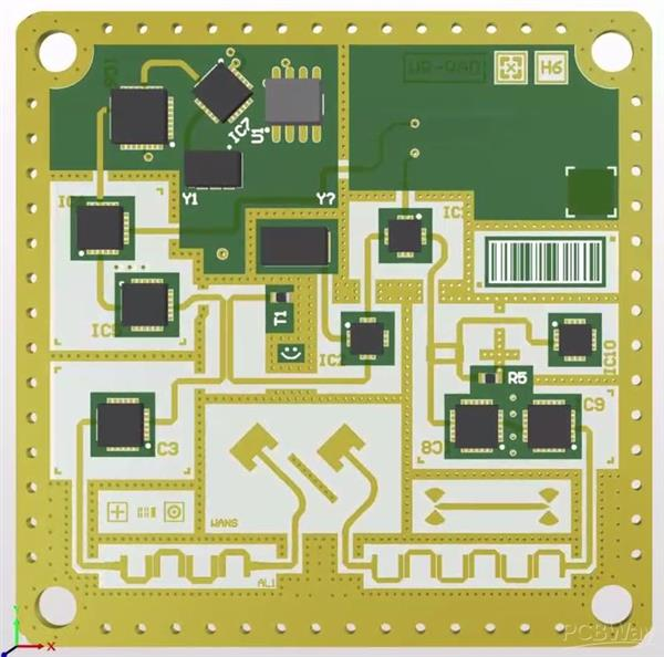
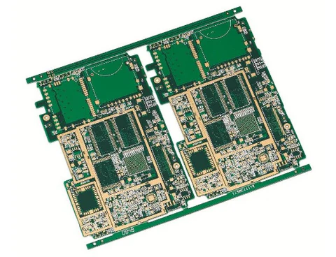
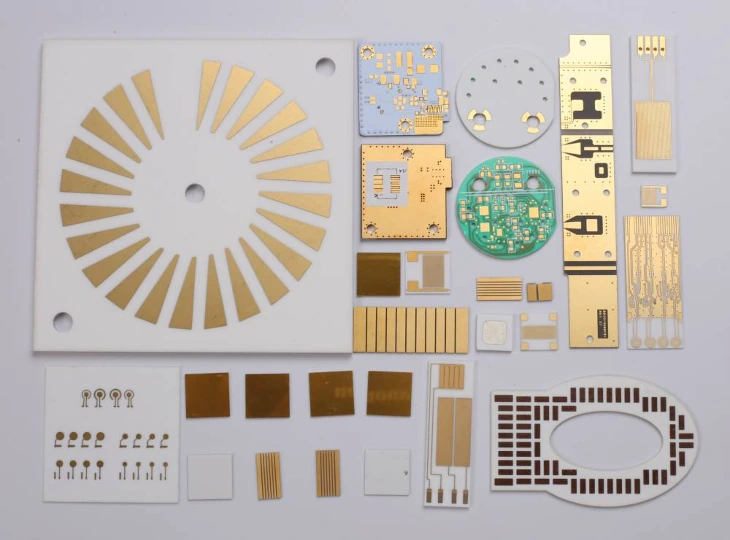
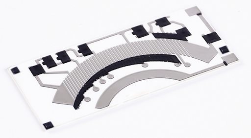
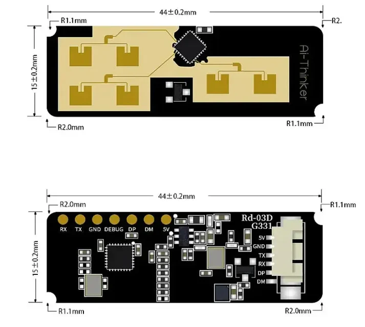
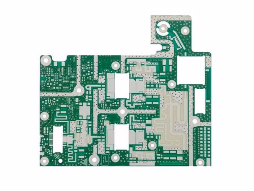
Automotive radar has become one of the most important sensing technologies in modern Advanced Driver Assistance Systems (ADAS) and autonomous driving platforms. By transmitting and receiving high-frequency electromagnetic signals, radar systems enable vehicles to accurately detect distance, speed, and object movement in complex environments. At the center of every high-performance radar module is the Automotive...