kkpcba-Cindy - KKPCB - Page 4 of 66
 
HomeAuthor

kkpcba-Cindy - KKPCB - Page 4 of 66

The Secrets of High-Frequency PCB Stack-Up Design: Importance, Principles, and Optimization Strategies

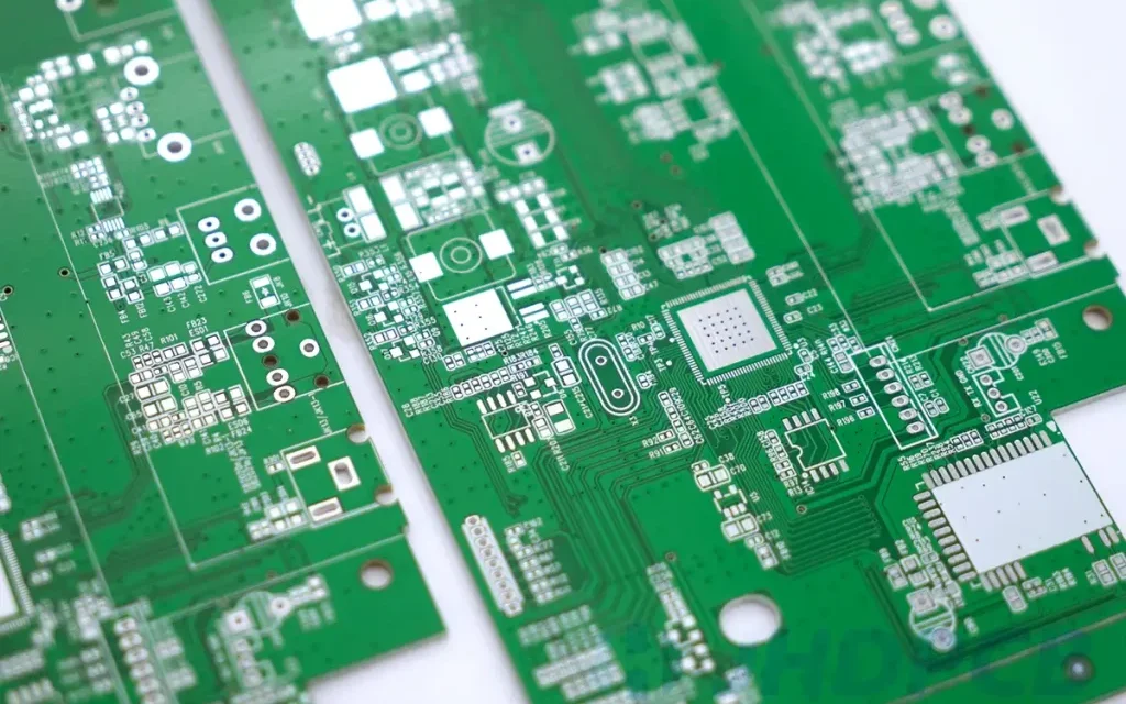
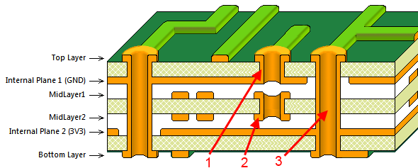
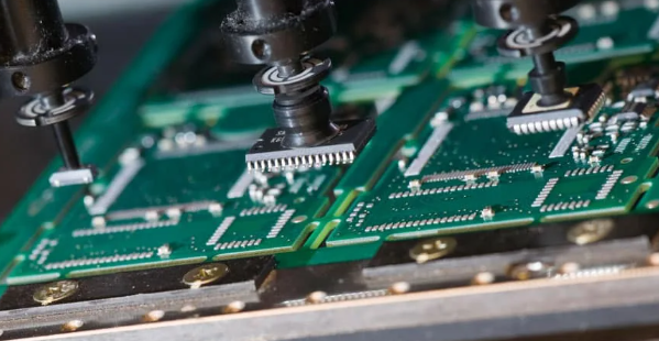
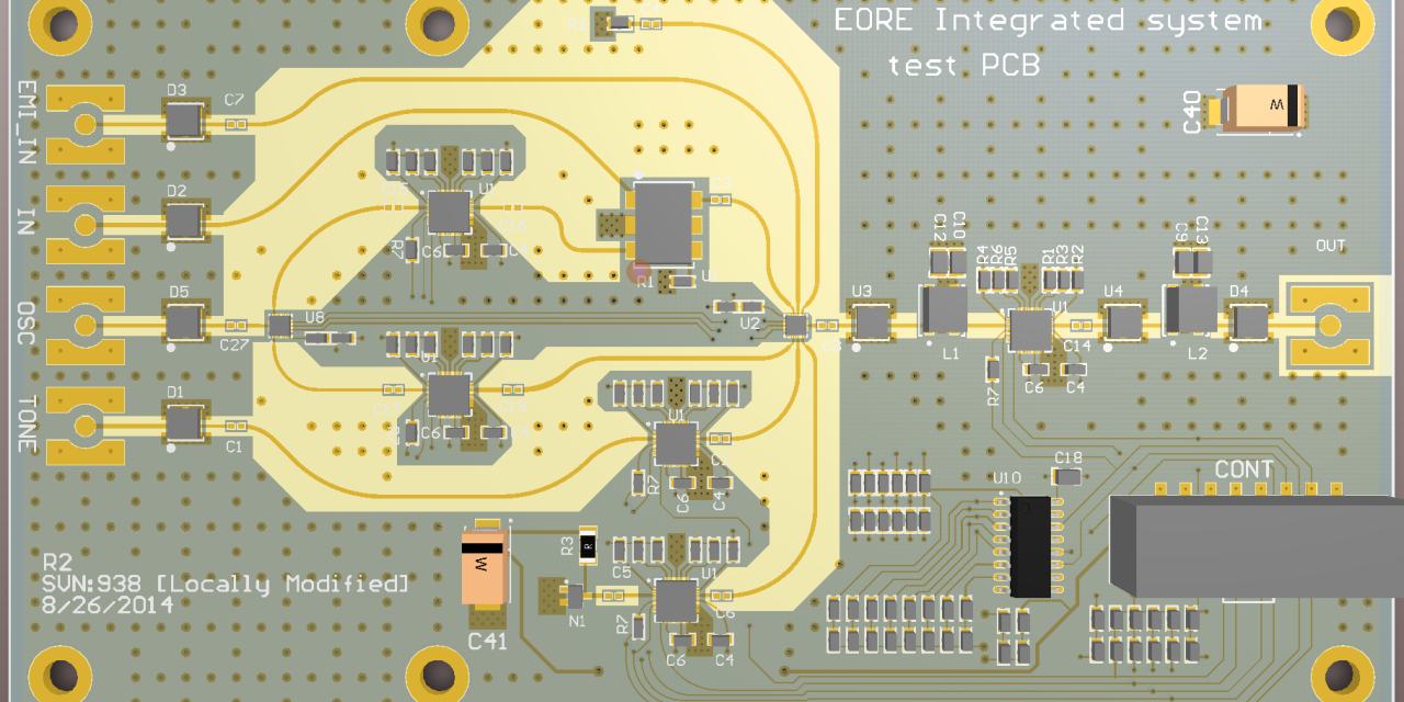
In high-speed and high-frequency electronic applications, RF PCB stack-up design plays a decisive role in ensuring stable performance, minimal signal loss, and electromagnetic compatibility. Proper PCB layer stack-up is not just a structural consideration—it directly determines signal integrity, impedance control, and overall product reliability. This article reveals the core principles of RF PCB stacking, explains...

Rigid-Flex Layered Design Explained

The Evolution of Modern PCB Interconnection Technology As electronic products continue evolving toward: smaller size lighter weight higher functionality greater reliability compact packaging traditional PCB structures often struggle to meet modern engineering requirements. Industries such as: aerospace electronics medical devices military systems wearable electronics automotive electronics robotics consumer electronics increasingly demand PCB solutions capable of:...

Solving the PCBA Processing Challenge: Causes, Hazards, and Ultimate Solutions for PCB Board Deformation

In the precision chain of modern electronics manufacturing, PCBA processing (Printed Circuit Board Assembly) serves as the critical stage that gives electronic products “life.” During this process, electronic components are precisely soldered onto a printed circuit board (PCB) to form a complete circuit system.However, PCB board deformation is a hidden issue that can severely affect...

How to Lay Out a Crystal Oscillator on a PCB

Why Crystal Oscillator Layout Is Critical The crystal oscillator (XTAL) is the timing reference of most electronic systems, including: Microcontrollers (MCUs) Microprocessors (MPUs) Communication modules RF systems Even though it operates at relatively low frequencies compared to RF circuits, the oscillator is extremely sensitive to noise, parasitics, and PCB layout quality. Improper layout can result...

PCB Design Guidelines for EMC Compliance

Why EMC Matters in PCB Design Electromagnetic Compatibility (EMC) is a key requirement in modern PCB design, ensuring that electronic systems operate reliably without generating or being affected by electromagnetic interference (EMI). Proper PCB layout—especially GND routing, trace spacing, and layer design—plays a decisive role in reducing ESD (Electrostatic Discharge) and improving overall signal integrity....

PCB Pad Soldering Processes Explained: Types, Features, and Selection Guide

Why PCB Pad Soldering Process Matters In PCB manufacturing, the pad surface finish or soldering process directly affects component solderability, electrical performance, and long-term reliability.Different processes offer varying degrees of oxidation resistance, flatness, and cost efficiency, making proper selection essential for every PCB design project. This article categorizes and compares the most common PCB pad...

Why Should Vias Be Staggered from Pad Positions in PCB Design?

 The Importance of Via Placement in PCB Design In PCB design, via positioning plays a crucial role in ensuring electrical performance, manufacturing reliability, and signal integrity. Improper via placement—especially placing vias directly on component pads—can lead to soldering defects, electrical noise, and higher production costs. This article explains why vias should be staggered from pad...

What are RSRP and RSRQ in 5G?

With the rapid development and widespread application of 5G technology, the field of wireless communication has ushered in unprecedented changes. In 5G networks, signal quality monitoring and evaluation are crucial for ensuring communication stability and reliability. Among them, Reference Signal Received Power (RSRP) and Reference Signal Received Quality (RSRQ) are two key performance indicators that play an...

Power supply noise is a common problem on high-frequency PCBs . This interference is usually caused by electromagnetic fields generated when current flows across the PCB. Electromagnetic fields are generated when current flows through power or ground lines on the PCB. If these fields interact with other components on the PCB, they can produce noise, thus affecting circuit performance....