Why Crystal Oscillator Layout Is Critical
The crystal oscillator (XTAL) is the timing reference of most electronic systems, including:
- Microcontrollers (MCUs)
- Microprocessors (MPUs)
- Communication modules
- RF systems
Even though it operates at relatively low frequencies compared to RF circuits, the oscillator is extremely sensitive to noise, parasitics, and PCB layout quality.
Improper layout can result in:
- Frequency instability
- Startup failure
- Increased phase noise
- Electromagnetic interference (EMI)
At KKPCB, crystal oscillator layout is optimized to ensure stable oscillation, low noise, and reliable long-term operation.
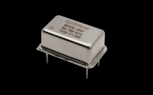
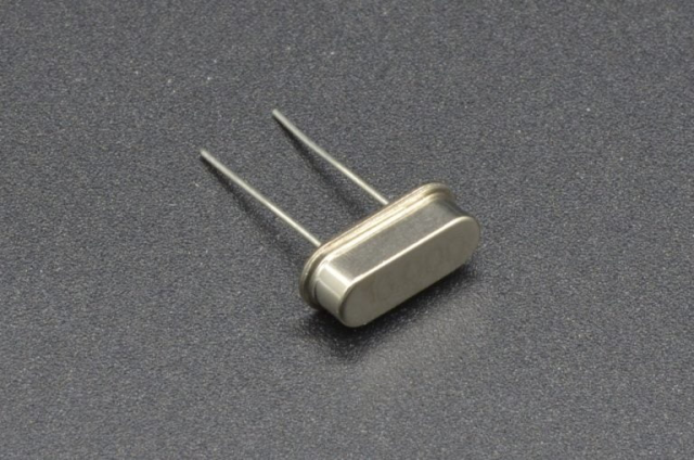
2. Basic Crystal Oscillator Circuit Structure
A typical crystal oscillator circuit includes:
- Crystal resonator
- Load capacitors (C1, C2)
- Oscillator pins (XTAL_IN / XTAL_OUT)
- Internal amplifier (inside MCU or IC)
The oscillation frequency depends on the crystal and load capacitance:
f=12πLCf = \frac{1}{2\pi\sqrt{LC}}f=2πLC1
Although simplified, this shows how parasitic capacitance and inductance can affect oscillation stability.
3. Key PCB Layout Rules for Crystal Oscillators
3.1 Place the Crystal Close to the MCU
This is the most important rule.
Best practice:
- Place the crystal as close as possible to the oscillator pins
- Keep traces extremely short and symmetrical
- Avoid routing through vias
Benefits:
- Reduces parasitic inductance and capacitance
- Improves startup reliability
- Minimizes noise coupling
3.2 Keep Crystal Traces Short and Symmetrical
Crystal signal traces should:
- Be as short as possible
- Have equal length (balanced routing)
- Avoid sharp corners
This ensures:
- Stable oscillation
- Balanced signal flow
- Reduced phase noise
3.3 Minimize Parasitic Capacitance and Inductance
Parasitics can detune the oscillator frequency.
Key actions:
- Avoid large copper areas near crystal traces
- Keep traces narrow and direct
- Avoid unnecessary vias
3.4 Proper Grounding for Noise Isolation
Grounding is critical for oscillator stability.
Best practices:
- Use a solid ground plane under the crystal
- Connect load capacitors directly to ground
- Avoid noisy return paths
In sensitive designs:
- Use a guard ring (ground ring) around the crystal
3.5 Load Capacitor Placement Optimization
Load capacitors (C1, C2) should be:
- Placed close to the crystal
- Connected with short traces
- Symmetrically arranged
This ensures:
- Accurate oscillation frequency
- Stable startup behavior
3.6 Isolate Crystal from High-Speed and Noisy Signals
Crystal circuits are highly sensitive to interference.
Avoid placing near:
- High-speed digital lines
- Switching power supplies
- RF transmission lines
Keep a dedicated quiet area for the oscillator.
3.7 Avoid Routing Under the Crystal
Routing signals beneath the crystal can introduce:
- Noise coupling
- EMI interference
Recommendation:
- Keep a keep-out area under the crystal
- Use ground plane shielding if necessary
3.8 Use Guard Ring for High-Precision Designs
For sensitive applications:
- Surround the crystal with a grounded guard ring
- Connect guard ring to ground plane
Benefits:
- Reduces EMI coupling
- Improves noise immunity
3.9 Power Supply Decoupling for Oscillator Circuit
Ensure clean power supply for the oscillator:
- Place decoupling capacitors near MCU power pins
- Use low-noise LDO regulators if required
- Isolate oscillator power from noisy circuits
3.10 Validate Oscillator Performance
After layout, verify:
- Oscillator startup time
- Frequency accuracy
- Signal waveform quality
Testing tools:
- Oscilloscope
- Frequency counter
- Spectrum analyzer
At KKPCB, validation includes:
- Oscillation stability testing
- EMI/EMC analysis
- Layout optimization feedback
4. Common Crystal Oscillator Layout Mistakes
Avoid these common errors:
- Crystal placed far from MCU
- Long or unbalanced traces
- Routing noisy signals nearby
- Improper grounding
- Incorrect load capacitor placement
These issues can cause:
- Oscillator failure
- Frequency drift
- System instability
5. Applications Requiring Stable Crystal Oscillator Layout
Crystal oscillator layout is critical in:
- Microcontroller-based systems
- Communication modules (UART, SPI, I2C timing)
- RF and wireless devices
- Automotive electronics
- Industrial control systems
6. Conclusion
Crystal oscillator PCB layout is a critical aspect of ensuring stable timing, low noise, and reliable system operation. Even small layout mistakes can significantly impact oscillator performance.
By following best practices in component placement, trace routing, grounding, noise isolation, and power integrity, engineers can achieve highly stable oscillator circuits.
With strong PCB design expertise, KKPCB provides optimized solutions for high-reliability clock circuits in modern electronic systems.
