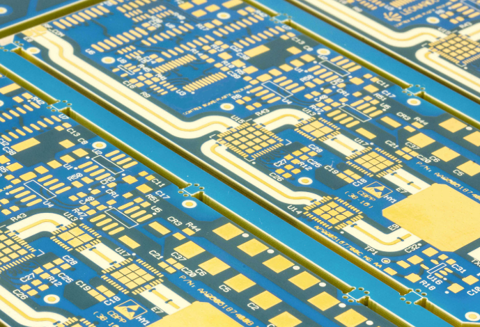
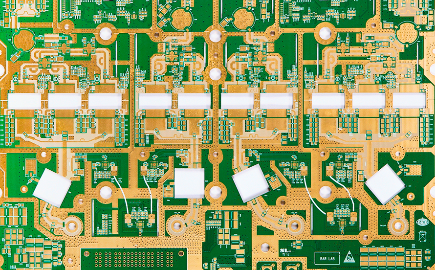
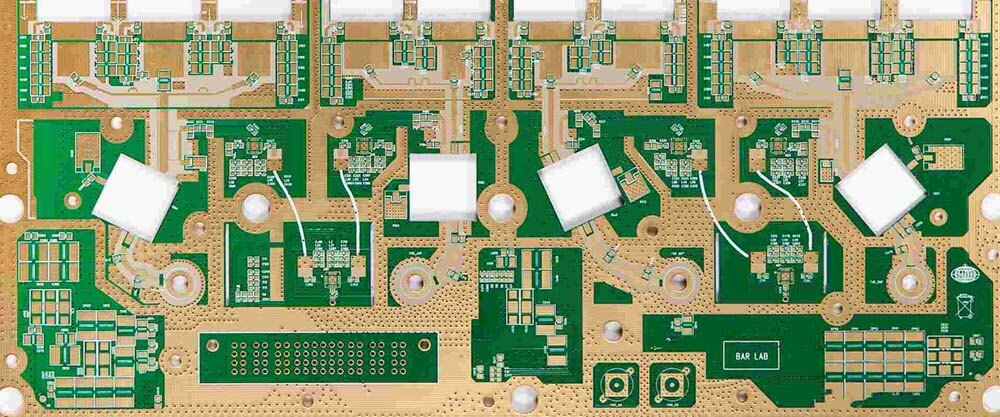
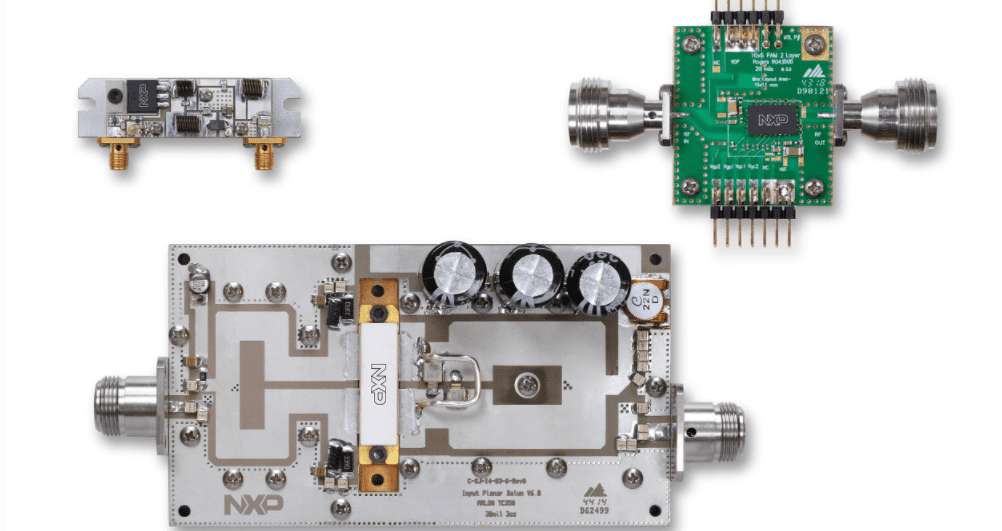
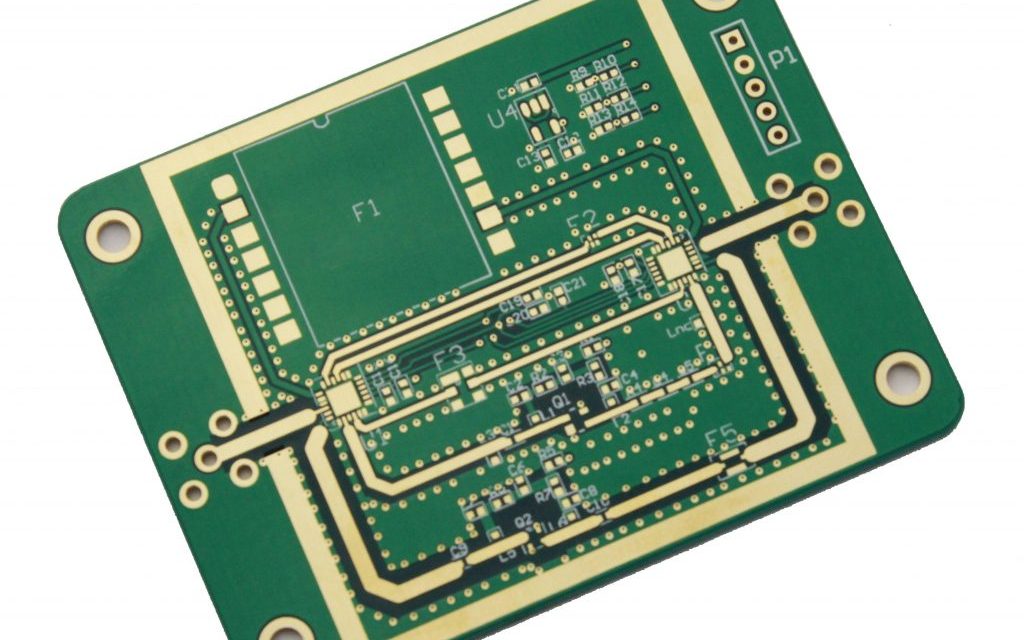
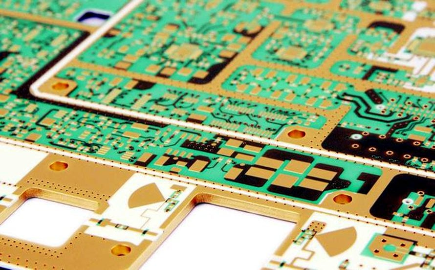
RF PCB design - KKPCB
 
HomeTag

RF PCB design - KKPCB

RF Trace PCB: Design Guidelines for Controlled Impedance & High-Frequency Signal Integrity

What is an RF Trace PCB? An RF Trace PCB refers to a printed circuit board specifically designed with controlled impedance traces to handle radio frequency (RF) signals. Unlike standard PCB routing, RF traces must maintain consistent electrical characteristics to avoid signal loss, reflection, and distortion. In RF design, the trace itself becomes part of...

RF Transceiver PCB: Key Design Technologies for Reliable Wireless Communication

In today’s connected world, RF transceiver PCB design plays a critical role in enabling stable and efficient wireless communication systems. From IoT devices to advanced communication infrastructure, high-performance RF PCB design ensures signal integrity, low interference, and reliable data transmission. Understanding the key design technologies behind RF transceiver PCBs is essential for achieving optimal performance....

Rogers PCB: High-Frequency PCB Materials for RF and Microwave Applications

Rogers PCB: High-Frequency PCB Materials for RF and Microwave Applications As wireless communication, radar systems, and high-frequency electronics continue to advance, traditional PCB materials such as standard FR-4 often struggle to meet performance requirements. Rogers PCB materials are specifically engineered to deliver superior electrical performance, low dielectric loss, and stable signal transmission at high frequencies....

RF Test PCB: Design Considerations for Accurate RF Circuit Testing

In radio frequency (RF) electronics, accurate signal measurement is essential for validating circuit performance. Before RF modules are integrated into final products, engineers typically use RF test PCBs to evaluate signal behavior, component functionality, and system stability. An RF test PCB is specifically designed to provide a controlled environment for testing high-frequency circuits. Proper design...

Rogers PCB: High-Frequency PCB Material for RF and Microwave Applications

As wireless communication technologies continue to evolve, electronic circuits must operate at increasingly higher frequencies. Traditional PCB materials such as standard FR4 often struggle to maintain signal integrity in high-frequency environments. This is why Rogers PCB materials have become a preferred choice for RF and microwave applications. Rogers laminates are engineered to provide stable electrical...

RF Trace PCB: Precision RF Routing for High-Frequency and Low-Loss Signal Transmission

An RF Trace PCB is a specialized printed circuit board designed for RF signal transmission and high-frequency applications, where signal loss, impedance stability, and EMI control are critical. As wireless technologies such as 5G, WiFi, GPS, IoT, and radar systems continue to grow, RF PCB performance requirements become stricter than ever. Unlike ordinary digital traces,...

Building Reliable High-Speed Electronics with Controlled Impedance PCB Architectures

Introduction: Why Controlled Impedance Defines High-Speed Reliability As high-speed electronics push into multi-gigabit data rates and high-frequency RF domains, signal behavior is no longer dominated by logic thresholds—it is governed by transmission line physics. In these systems, every PCB trace behaves as a controlled impedance structure, and any deviation can introduce reflections, timing skew, and...

Engineering Low Dissipation Factor PCBs for High-Frequency and RF Performance

1. Engineering Context  As electronic systems push into higher frequencies—5G, mmWave sensing, radar, satellite communication, and precision instrumentation—the dissipation factor (Df) of PCB materials has become a primary performance determinant.A Low Dissipation Factor PCB minimizes dielectric loss, preserves signal integrity, and ensures stable operation at frequencies where traditional FR-4 rapidly degrades. Low Df PCBs bridge...

Achieve Low-Loss Transmission and Stable Impedance Performance with Double Layer HF PCB Engineering for High-Frequency Communication Systems

A Double Layer HF PCB may appear structurally simple, yet in high-frequency engineering it provides a remarkably efficient platform for low-loss propagation, stable impedance, and predictable electromagnetic behavior. When RF designers need high-frequency stability without the cost or stackup escalation of multilayer PCBs, a Double Layer HF PCB offers the ideal balance between manufacturability and...

Enhance Electromagnetic Uniformity and Mode-Suppression Using RT/duroid 5880 PCB Stackups in Precision mmWave Routing Networks

Precision mmWave systems increasingly depend on PCB materials that can maintain electromagnetic uniformity, suppress parasitic modes, and control insertion loss across wideband operating ranges. RT/duroid 5880 PCB stackups have become a leading choice for these environments because their low dielectric constant, low-loss tangent, and exceptional stability under thermal and mechanical stress allow engineers to design...