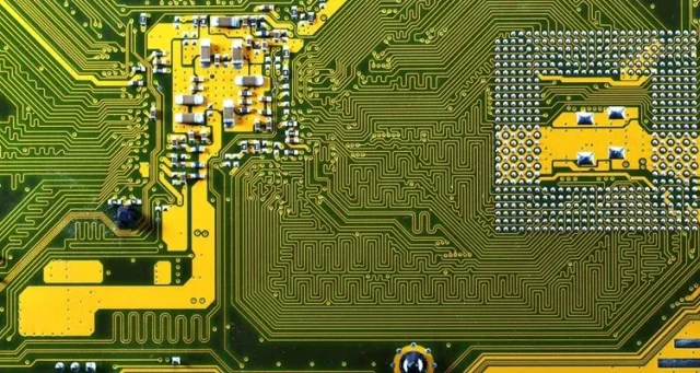
1. Introduction to Impedance Controlled PCB
As modern electronic systems continue advancing toward:
- Higher frequencies
- Faster data transmission
- Higher signal density
traditional PCB routing methods are no longer sufficient to guarantee stable signal transmission.
In applications such as:
- 5G communication systems
- High-speed servers
- Automotive radar
- RF and microwave electronics
- Aerospace communication systems
Impedance Controlled PCB design has become a critical requirement for maintaining:
- Signal integrity
- Low signal loss
- Stable transmission quality
At KKPCB, advanced impedance-controlled PCB solutions are engineered for high-speed and high-frequency electronic applications.
2. What Is an Impedance Controlled PCB?
An impedance controlled PCB is a printed circuit board designed to maintain a specific characteristic impedance value throughout signal transmission paths.
Controlled impedance ensures:
- Minimal signal reflection
- Stable waveform transmission
- Reduced EMI and crosstalk
3. Why Controlled Impedance Is Important
Without proper impedance control:
- Signal reflections increase
- Data transmission errors occur
- High-frequency performance degrades
Controlled impedance PCB technology improves:
- High-speed signal stability
- RF transmission efficiency
- System reliability
This is especially critical for:
- DDR memory routing
- PCIe interfaces
- USB and HDMI systems
- RF antennas and microwave circuits
4. Key Factors Affecting PCB Impedance
4.1 PCB Stack-Up Design
Impedance depends heavily on:
- Dielectric thickness
- Layer spacing
- Ground plane arrangement
A properly optimized stack-up improves:
- Signal return paths
- EMI suppression
- Transmission consistency
4.2 PCB Material Selection
Low-loss PCB materials provide:
- Stable dielectric constant (Dk)
- Reduced insertion loss
- Better high-frequency performance
Common materials include:
- FR4 High-Speed Materials
- Rogers Laminates
- PTFE PCB Materials
4.3 Trace Width and Copper Thickness
Signal impedance changes with:
- Trace geometry
- Copper thickness
- Distance to reference plane
Precision manufacturing is required for accurate impedance control.
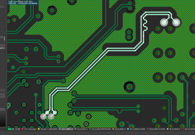
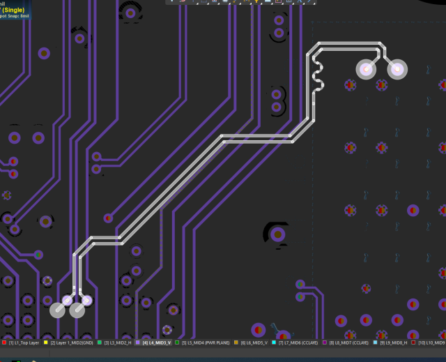
4.4 Differential Pair Routing
Differential signals require:
- Controlled spacing
- Length matching
- Symmetrical routing
This improves:
- Noise immunity
- Signal integrity
- EMI performance
5. PCB Transmission Line Structures
Common impedance-controlled structures include:
Microstrip
- Routed on outer layers
- Easy fabrication
- Good RF performance
Stripline
- Embedded between ground planes
- Better EMI shielding
- Stable impedance consistency
Coplanar Waveguide
- Common in RF and microwave PCB design
- Excellent high-frequency performance
6. Signal Integrity Challenges in High-Speed PCB Design
Controlled impedance PCB design helps reduce:
- Signal reflection
- Ringing
- Crosstalk
- Timing skew
Signal quality becomes increasingly important as data rates continue rising.
At KKPCB, advanced simulation and impedance optimization ensure stable high-frequency signal transmission.
7. Manufacturing Requirements for Impedance Controlled PCB
High-precision manufacturing is essential for:
- Accurate trace width control
- Consistent dielectric thickness
- Stable copper etching processes
Key manufacturing technologies include:
- Laser direct imaging (LDI)
- Automated optical inspection (AOI)
- Controlled lamination processing
- TDR impedance testing
8. Impedance Testing and Quality Control
PCB impedance verification methods include:
- Time Domain Reflectometry (TDR)
- Impedance test coupons
- High-frequency signal analysis
These tests ensure:
- Consistent impedance values
- Reliable electrical performance
- Stable production quality
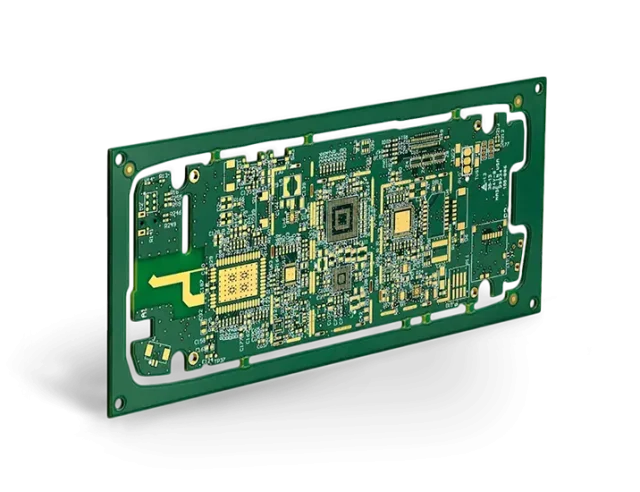
9. Applications of Impedance Controlled PCB
Impedance-controlled PCBs are widely used in:
- 5G base stations
- High-speed networking equipment
- RF amplifiers
- Automotive radar systems
- Aerospace communication modules
- Medical imaging electronics
These applications require:
- High signal accuracy
- Low transmission loss
- Excellent EMI performance
10. Future Trends in Impedance Controlled PCB Technology
Future PCB technologies are evolving toward:
- Higher data bandwidth
- mmWave communication
- AI server infrastructure
- Ultra-low-loss PCB materials
Advanced impedance-controlled PCB solutions will increasingly require:
- Low-profile copper foil
- Advanced RF laminates
- Ultra-precise manufacturing processes
11. Conclusion
Impedance Controlled PCB technology is essential for modern:
- High-speed digital electronics
- RF and microwave systems
- Advanced communication infrastructure
Through optimized stack-up design, precision routing, and advanced manufacturing control, engineers can achieve:
- Superior signal integrity
- Stable impedance performance
- Reliable high-frequency operation
With extensive expertise in high-speed PCB engineering, KKPCB delivers advanced PCB solutions for next-generation electronic systems.
