
As electronic products continue to evolve toward smaller form factors and higher performance, conventional PCB technologies often reach their limits. The HDI PCB (High-Density Interconnect PCB) overcomes these limitations by enabling ultra-dense routing, shorter signal paths, and enhanced electrical performance.
A professionally engineered HDI PCB is essential for modern high-speed and high-density electronic systems.
What Is an HDI PCB?

An HDI PCB is a printed circuit board that incorporates advanced interconnect technologies such as:
-
Laser-drilled microvias
-
Fine-line trace and space
-
Sequential lamination
These features significantly increase routing density compared to traditional PCBs.
Why HDI PCB Technology Matters
HDI PCBs are widely adopted because they:
-
Support high pin count components
-
Reduce board size and layer count
-
Improve electrical performance
HDI technology enables compact designs without compromising reliability.
Microvia Structures and Interconnect Design
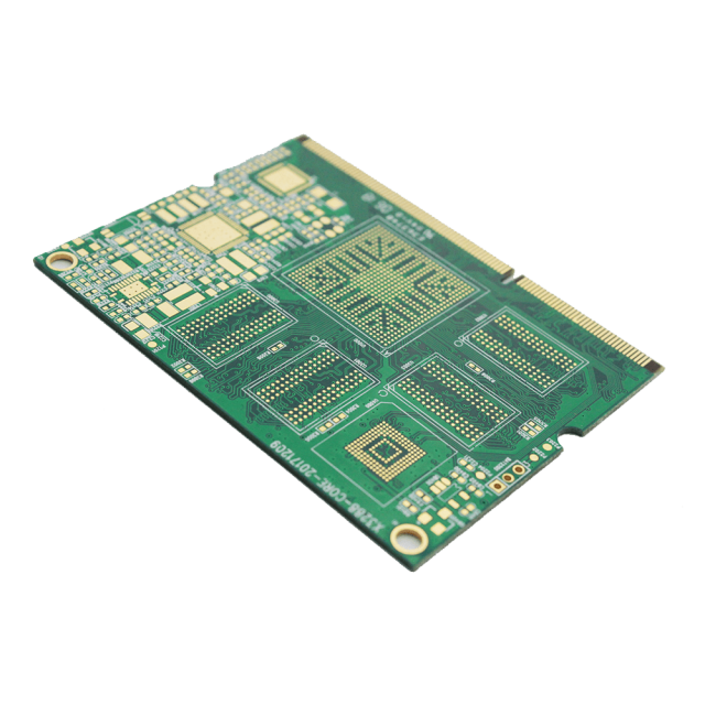
Microvias are the core of HDI PCB technology. Common structures include:
-
Blind microvias
-
Buried microvias
-
Stacked and staggered microvias
These structures enable efficient signal breakout and routing.
Fine-Line Routing for High-Speed Signals
HDI PCBs support extremely fine trace widths and spacing, allowing:
-
Dense signal routing
-
Improved impedance control
-
Reduced signal path length
Shorter paths help maintain signal integrity at high speeds.
Signal Integrity Advantages of HDI PCBs
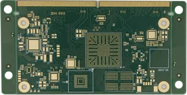
HDI technology improves signal integrity by:
-
Minimizing via stubs
-
Reducing parasitic capacitance and inductance
-
Enhancing return path continuity
These benefits are critical for high-speed digital and RF designs.
Power Integrity and Decoupling Optimization
Compact layouts increase power integrity challenges. HDI PCBs address this by:
-
Placing decoupling capacitors close to devices
-
Using low-inductance power paths
-
Optimizing plane structures
Stable power delivery supports reliable system operation.
Material Selection and Stackup Design
HDI PCBs commonly use:
-
High-Tg FR-4 for structural stability
-
Low-loss materials for high-speed layers
-
Symmetrical stackups to control warpage
Material selection balances performance, cost, and manufacturability.
Manufacturing Challenges and Process Control
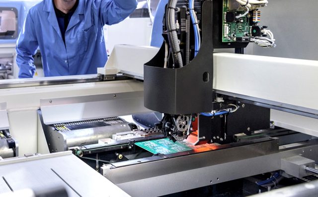
HDI PCB fabrication requires:
-
Precise laser drilling
-
Reliable via filling and planarization
-
Accurate layer-to-layer registration
Strict process control ensures high yield and consistency.
Typical Applications of HDI PCBs
HDI PCBs are widely used in:
-
Smartphones and consumer electronics
-
High-speed computing and networking systems
-
Medical and automotive electronics
-
Semiconductor test and advanced modules
These applications demand compact size and high performance.
Choosing an HDI PCB Manufacturer
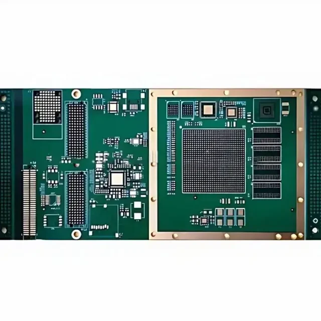
When selecting an HDI PCB supplier, consider:
-
Experience with microvia and sequential lamination
-
Fine-line manufacturing capability
-
Controlled impedance and electrical testing support
-
Engineering collaboration during design review
A skilled manufacturer ensures reliable HDI PCB production.
Conclusion
The HDI PCB is a key enabler of compact, high-speed, and high-density electronic designs. Through microvia technology, fine-line routing, and precise manufacturing, HDI PCBs deliver superior electrical performance and design flexibility.
Partnering with an experienced HDI PCB manufacturer ensures consistent quality from prototype to mass production.

