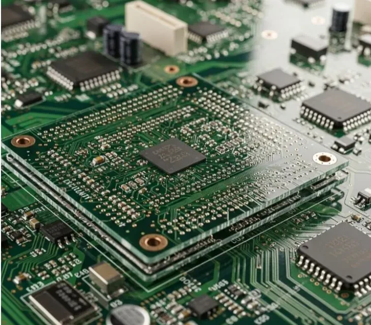
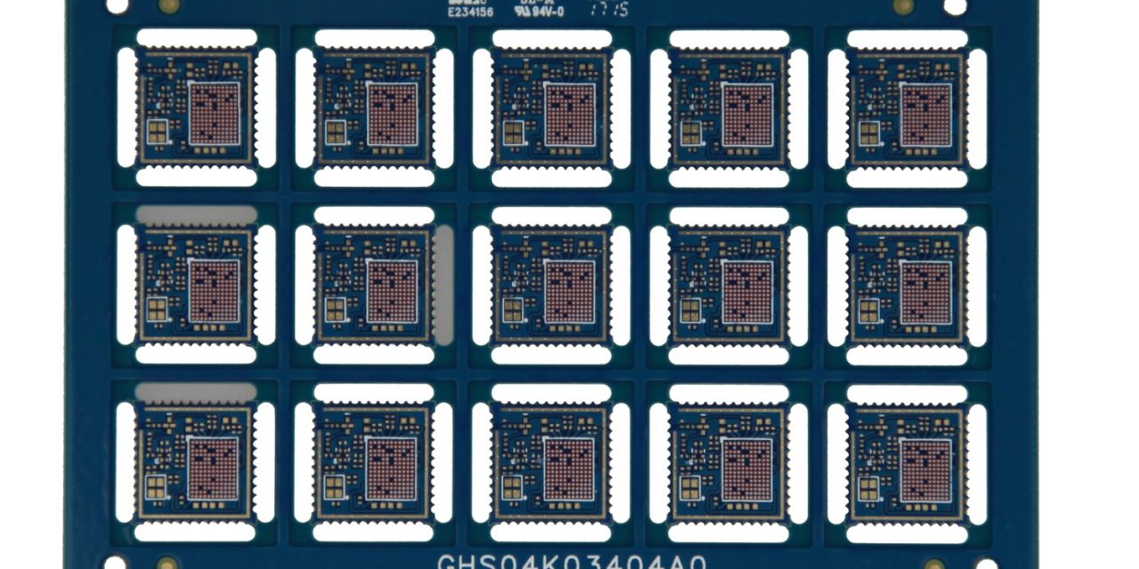
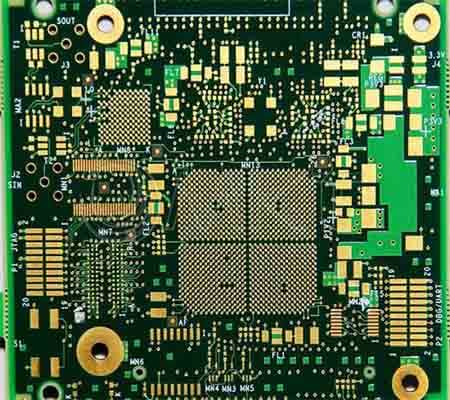
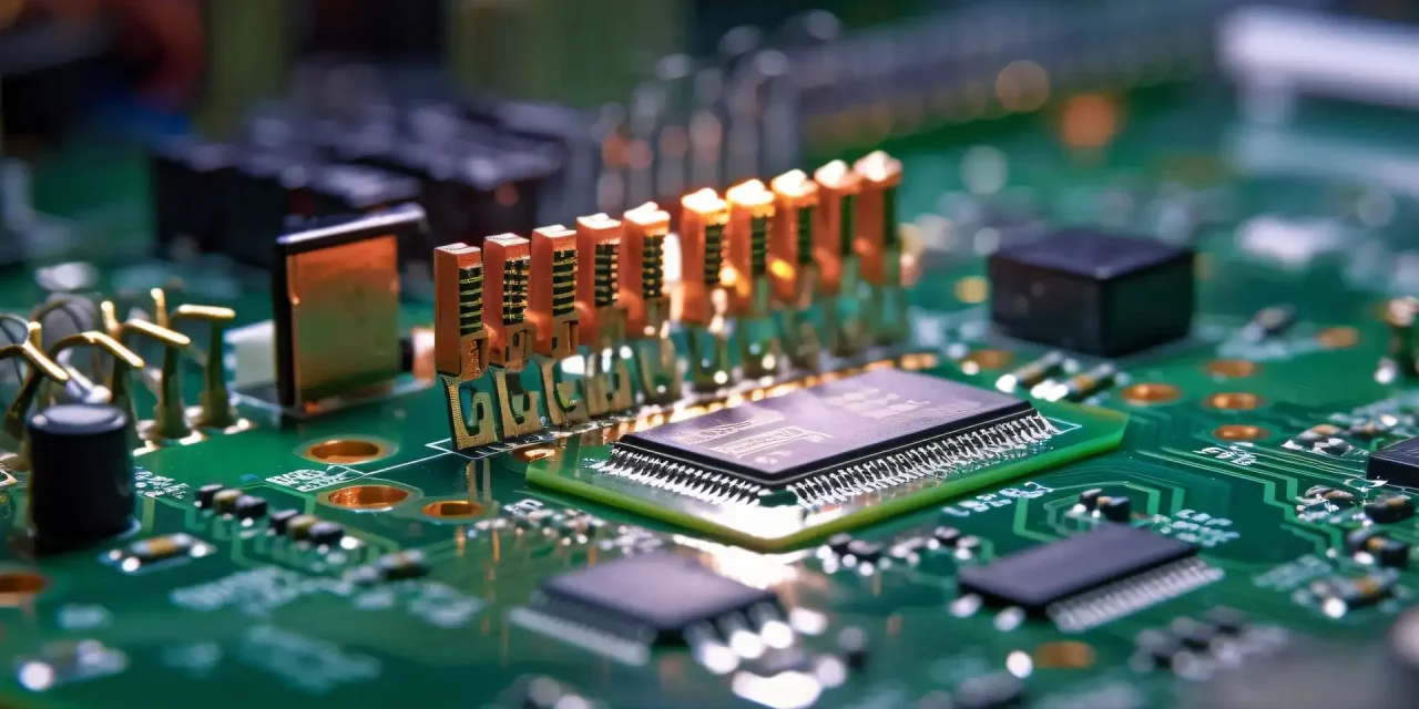
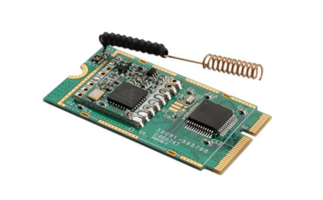
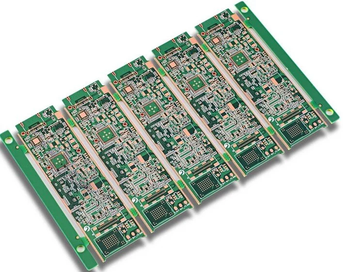
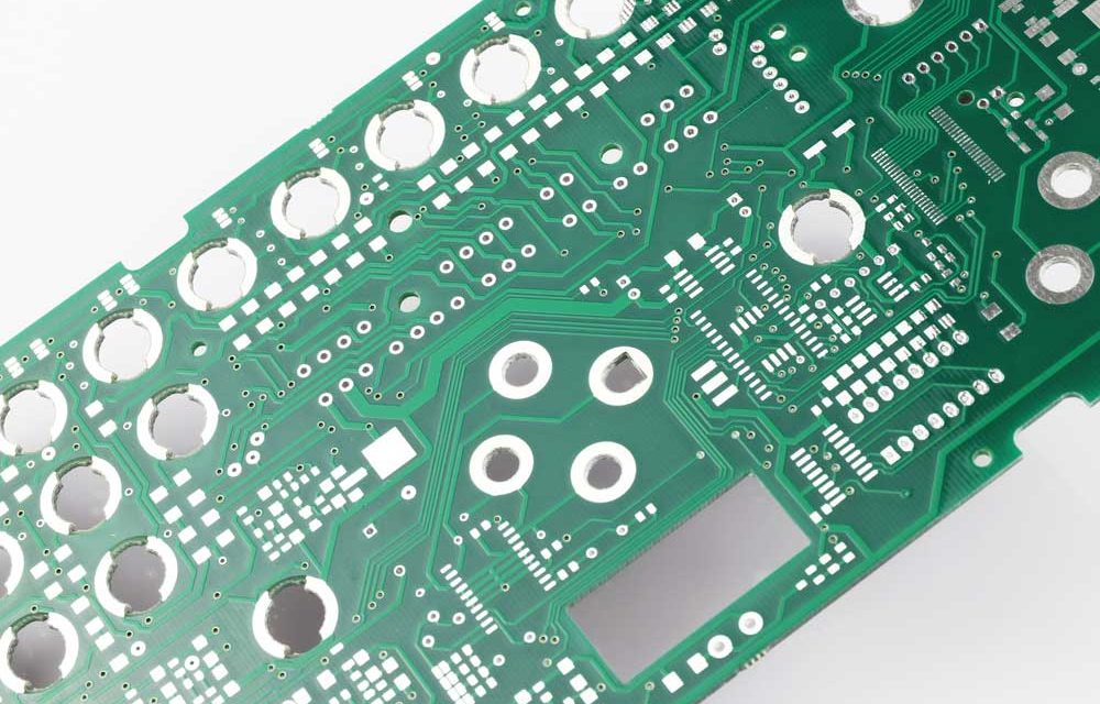
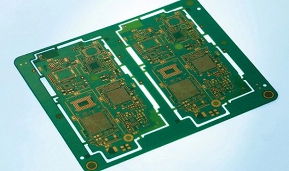
Microvia PCB - KKPCB
 
HomeTag

Microvia PCB - KKPCB

High Density PCB Design – Engineering Solutions for Complex and Compact Electronic Systems

Engineering Challenges Behind High Density PCB As electronic systems become more compact and functionally integrated, PCB designers are facing increasing layout complexity. A High Density PCB is not simply about placing more components on a board — it requires precise coordination between electrical design, stack-up engineering, manufacturability, and long-term reliability. High density PCB development focuses...

HDI PCB – High Density Interconnect PCB for Advanced Electronic Applications

What Is an HDI PCB? An HDI PCB (High Density Interconnect PCB) is a printed circuit board designed with higher wiring density per unit area compared to traditional PCBs. It typically incorporates microvias, blind and buried vias, fine trace widths, and advanced multilayer stack-ups to support compact and high-performance electronic designs. HDI technology enables smaller...

Microvia PCB – High Density Interconnect PCB for Advanced Electronic Applications

Microvia PCB for High Density Interconnect (HDI) Design As electronic products continue to shrink in size while increasing in functionality, traditional through-hole PCB structures are no longer sufficient. Microvia PCB technology enables higher routing density, improved signal integrity, and compact multilayer stackups, making it essential for modern high-performance electronics. Microvias are laser-drilled vias typically with...

Fine Pitch PCB – Precision PCB for High Density and Fine Line Applications

What Is Fine Pitch PCB? A Fine Pitch PCB refers to a printed circuit board designed with extremely small trace width and spacing to support high pin count and fine pitch components. It is commonly used in advanced electronic systems where compact design, high integration, and precise routing are essential. Fine pitch designs are typically...

IoT IC Test PCB – High Precision PCB for IoT Chip Testing Applications

What Is an IoT IC Test PCB? An IoT IC Test PCB is a specialized printed circuit board used for validating and testing integrated circuits (ICs) designed for Internet of Things (IoT) applications. These PCBs are commonly used in semiconductor test environments such as: Automated Test Equipment (ATE) systems Load boards Probe card assemblies Burn-in...

HDI PCB – High Density Interconnect PCB for Advanced Electronics

What Is HDI PCB? HDI PCB (High Density Interconnect PCB) is a printed circuit board designed with higher wiring density per unit area compared to traditional multilayer PCBs. It uses advanced manufacturing technologies such as microvias, blind vias, buried vias, and fine line traces to achieve compact size and improved electrical performance. HDI PCB is...

Blind Via PCB – High Density Interconnect PCB for Compact and High Speed Designs

What Is a Blind Via PCB? A Blind Via PCB is a type of printed circuit board that contains vias connecting internal layers to one or more outer layers without passing completely through the board. Unlike through-hole vias, blind vias help: Reduce board size Increase routing density Optimize multilayer stack-ups Support HDI (High Density Interconnect)...

BT Epoxy PCB Manufacturing for IC Substrate and High Density Applications

What Is a BT Epoxy PCB? A BT Epoxy PCB is a high-performance printed circuit board manufactured using Bismaleimide Triazine (BT) resin-based epoxy material. BT Epoxy PCB is widely used in IC substrate applications, semiconductor packaging, memory modules, and high-density electronic devices, where thermal stability, dimensional accuracy, and electrical performance are critical. Compared with standard...

PTFE PCB Manufacturing for High-Frequency and RF Applications

What Is a PTFE PCB? A PTFE PCB is a printed circuit board made from polytetrafluoroethylene (PTFE) laminates, known for extremely low dielectric loss, stable dielectric constant, and excellent high-frequency performance. PTFE PCBs are widely used in 5G, mmWave modules, RF/microwave systems, aerospace electronics, and high-speed computing, where signal integrity and low insertion loss are...

Rogers PCB Manufacturing for High-Frequency and RF Applications

What Is a Rogers PCB? A Rogers PCB is a printed circuit board that uses Rogers high-frequency laminates, such as RO4003C, RO4350B, and Duroid series, designed for low dielectric loss, precise impedance control, and high-frequency signal transmission. Rogers PCBs are essential in 5G communications, RF/microwave modules, high-speed computing, and aerospace electronics. Why Rogers PCB Technology...