HomeTag

high-frequency PCB - KKPCB

Improve Wideband Isolation and EMI Suppression Using Engineered 5G Router PCB Layouts for CPE Systems

Customer-Premises Equipment (CPE) sits at the frontline of the 5G access network. Unlike traditional routers, a 5G CPE must simultaneously maintain wideband RF isolation, suppress broadband EMI, and stabilize the 2.4 GHz / 5 GHz / 6 GHz multi-band wireless channels while handling dense digital switching activity. At these frequencies, the PCB layout is no...
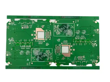
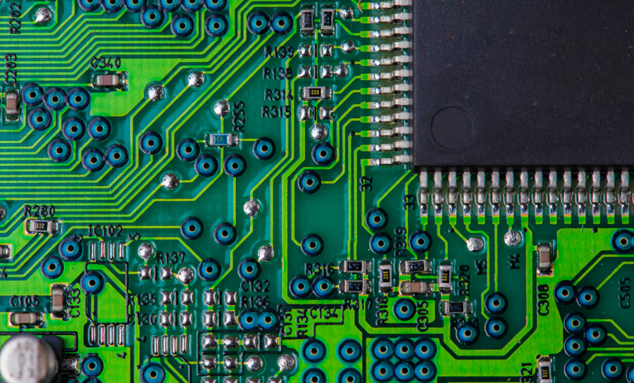
Optimize Signal Integrity and Multi-Band RF Stability with 5G Router PCB Architectures Using Low-Loss Materials

Next-generation 5G routers operate across 2.4, 5, and 6 GHz bands while supporting high-speed MIMO data streams and concurrent RF channels. Maintaining signal integrity, low insertion loss, and impedance accuracy across multilayer PCB architectures is critical for throughput, link stability, and network reliability. Low-loss PCB laminates (Dk ~3.0 ±0.04, Df ~0.0012 @10 GHz) provide minimal...

Enhance Wideband Signal Integrity and Suppress Mode Conversion with Multilayer HF PCB Stackups for Next-Generation RF Sensing Architectures

Next-generation RF sensing architectures, including automotive ADAS radar modules, industrial LiDAR, and high-resolution environmental sensors, demand wideband signal fidelity, minimal mode conversion, and low insertion loss across multilayer PCB interconnects. Phase stability and impedance accuracy are critical to ensure precise beamforming, timing synchronization, and high-speed data acquisition. Multilayer HF PCB laminates with controlled dielectric properties...

Achieve High-Frequency Channel Reliability and Precision Impedance Control with Megtron 7 PCB Stackups in Advanced Server Motherboards

Modern high-performance server motherboards handle multi-gigabit data streams across PCIe Gen5/Gen6, DDR5 memory, and high-speed interconnects. Ensuring channel reliability, minimal signal attenuation, and precise impedance control is critical to maintain data integrity, low bit error rates (BER), and thermal stability in dense server environments. Megtron 7 PCB laminates (Dk = 3.4 ± 0.03, Df =...

Drive Ultra-Clean Electromagnetic Performance Through Precision-Aligned Multilayer HF PCB Dielectrics in Wideband Radar Processing Units

Wideband radar processing units operating in 8–40 GHz and beyond require multilayer HF PCBs with precisely aligned dielectric layers to maintain ultra-clean electromagnetic performance. Signal integrity, insertion loss, and phase stability are critically sensitive to stackup alignment, trace spacing, and dielectric uniformity. KKPCB leverages precision-laminated multilayer HF PCB substrates, low-roughness copper, and impedance-calibrated routing to...

Reduce Insertion Loss and Boost Antenna Performance with Next-Gen 5G Router PCB Platforms

Next-generation 5G router PCB engineering is reshaping the performance limits of consumer and enterprise wireless systems. As 5G routers, gateways, mesh nodes, and outdoor CPE units push into wider sub-6 GHz and emerging FR1/FR2 ranges, the PCB becomes far more than a mechanical carrier—it is the decisive RF medium that determines insertion loss, antenna efficiency,...

Achieve Ultra-Consistent Dk/Df Performance Through RO4835 PCB Engineering for 5G Massive-MIMO Radio Units

The Importance of Dk/Df Stability in 5G Systems As 5G communication systems continue to evolve, especially in Massive MIMO radio units, maintaining ultra-consistent dielectric constant (Dk) and dissipation factor (Df) is critical for ensuring stable RF performance and reliable high-speed signal transmission. In high-frequency RF PCB design, even small variations in Dk/Df performance can lead...

Impedance Matching in HDI PCB Design

In modern HDI PCB design (High-Density Interconnect PCB design), achieving precise impedance matching is essential for maintaining signal integrity, minimizing reflection, and ensuring high-speed signal transmission. As data rates increase and circuit density grows, impedance control in HDI PCB layout becomes more complex due to fine trace geometries, microvias, and multilayer stack-ups. Effective impedance matching...

Enhance Thermal Reliability and High-Power RF Efficiency Through Advanced 5G Router PCB Stackups

5G router PCB platforms operate under multi-band RF loads, high-density routing, and continuous thermal cycling in compact CPE enclosures. Achieving stable RF efficiency requires a stackup engineered around low-loss materials, controlled dielectric stability, and carefully optimized thermal paths. This article analyzes how engineered 5G router PCB stackups improve RF efficiency, insertion-loss performance, and long-term thermal...

Low Loss PCBs Explained: Materials, Features & High-Frequency Performance

What Is a Low Loss PCB? Premium Materials, Performance Advantages & Applications In high-frequency electronics, signal integrity is everything. As data rates climb and RF systems move into the mmWave range, traditional FR-4 PCBs quickly become inadequate due to excessive dielectric loss, copper loss and thermal instability. At KKPCB, we engineer Low Loss PCBs specifically...