High Frequency PCB Design - KKPCB
 
HomeTag

High Frequency PCB Design - KKPCB

High Frequency Signal PCB: Design Principles for Reliable RF and High-Speed Applications

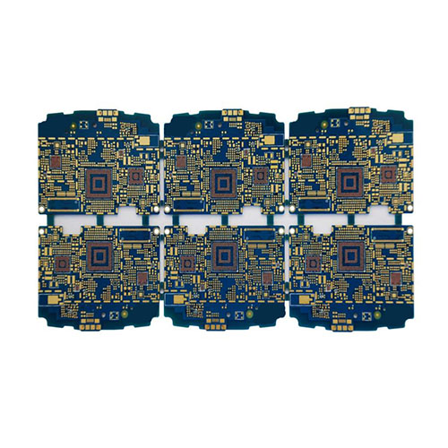
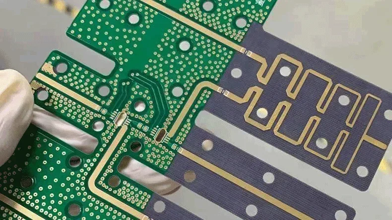
High Frequency Signal PCB: Design Principles for Reliable RF and High-Speed Applications With the rapid development of wireless communication, radar systems, and high-speed digital electronics, High Frequency Signal PCB design has become increasingly critical. Signals operating in the GHz range are highly sensitive to impedance mismatches, dielectric loss, electromagnetic interference (EMI), and routing discontinuities. Therefore,...

Taconic PCB: High-Frequency PCB Materials for RF and Microwave Applications

As wireless technologies continue to advance, high-frequency electronic circuits require PCB materials with stable electrical properties and low signal loss. Taconic PCBs are widely used in RF and microwave applications because they provide excellent dielectric performance and reliable signal transmission at high frequencies. Taconic laminates are specifically engineered to support high-speed and high-frequency circuits, making...

High Frequency PCB ODM: End-to-End Design and Manufacturing Solutions for RF and Microwave Applications

A professional High Frequency PCB ODM provides complete, end-to-end solutions covering PCB design, material selection, fabrication, and validation for RF, microwave, and high-speed electronic systems. As frequencies continue to increase in applications such as 5G communication, mmWave modules, radar systems, and high-speed networking, traditional PCB manufacturing alone is no longer sufficient. High frequency PCB ODM...

Achieve Ultra-Consistent Dk/Df Stability Using RO4835 PCB Architectures for High-Density 5G Massive-MIMO Radio Units

Next-generation 5G massive-MIMO radio units require high-density PCB designs that maintain ultra-consistent dielectric constant (Dk) and dissipation factor (Df) across all layers. Any variation in Dk/Df can lead to impedance mismatches, phase errors, and RF signal degradation, negatively affecting beamforming accuracy and spectral efficiency. RO4835 PCB laminates (Dk = 3.48 ± 0.03, Df = 0.0037...

Reinforce Shock Reliability and High-Frequency Integrity Through Ruggedized mmWave Module PCB Designs for Harsh-Environment Communication Terminals

Harsh-environment communication terminals—used in battlefield radios, mining telemetry units, emergency response networks, and remote industrial gateways—depend on mmWave Module PCB architectures that can preserve signal integrity, impedance accuracy, and structural reliability under extreme stress. High-frequency circuits operating from 24 GHz to 71 GHz experience sensitivity far greater than conventional RF PCB designs, making material stability,...

Achieve Ultra-Stable Dk/Df and Low-Loss Performance with RO4835 PCB Architectures for High-Density 5G Massive-MIMO Radio Units

Next-generation 5G massive-MIMO radio units require high-density PCB designs that maintain ultra-consistent dielectric constant (Dk) and dissipation factor (Df) across all layers. Any variation in Dk/Df can lead to impedance mismatches, phase errors, and RF signal degradation, negatively affecting beamforming accuracy and spectral efficiency. RO4835 PCB laminates (Dk = 3.48 ± 0.03, Df = 0.0037...

Optimizing High-Frequency Stability and Low-Loss Transmission Using RF-35 PCB Laminates for Modern Wireless Systems

As modern wireless systems continue to evolve toward higher frequencies and faster data rates, achieving high-frequency stability and low-loss signal transmission has become a critical requirement in RF PCB design. One of the most effective ways to optimize high-frequency PCB performance is through advanced material selection—specifically RF-35 PCB laminates. RF-35 laminates are engineered for high-frequency...

RF Testing and Reliability Evaluation of RO4350B PCBs for High-Frequency Modules

As high-frequency modules continue to evolve in RF communication, radar, and 5G systems, ensuring the performance and durability of RO4350B PCBs has become a critical aspect of RF PCB design and manufacturing. RO4350B PCB laminates, widely used in high-frequency PCB applications, offer low dielectric loss, stable dielectric constant, and excellent thermal performance. However, achieving optimal...

RO4350B PCB Hybrid Stackup Design and Lamination Challenges in Mass Production

As high-frequency PCB design becomes increasingly prevalent in RF, 5G, and high-speed digital systems, the use of RO4350B PCB materials in combination with standard FR4 has led to the widespread adoption of hybrid PCB stackup design. A RO4350B hybrid stackup PCB enables designers to balance cost efficiency and high-frequency performance, making it ideal for complex...

HDI PCB Technology Explained: Advanced High-Density Interconnect Solutions for Next-Gen Electronics

As modern electronics evolve toward smaller, faster, and more powerful systems, High-Density Interconnect (HDI) PCB technology has become the backbone of next-generation product design.As a professional one-stop PCB and PCBA solution provider, KKPCB is committed to delivering high-performance HDI printed circuit boards that meet the increasing demands for miniaturization, precision, and reliability in today’s electronics...