HomeTag

HDI PCB - KKPCB

HDI PCBs: Unlocking High-Density Performance for Modern Electronics

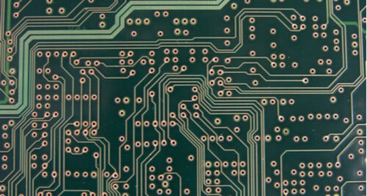
High-Density Interconnect (HDI) PCBs are a key technology for today’s compact and high-performance electronics. With fine lines, microvias, blind and buried vias, and multiple layers, HDI PCBs allow designers to fit complex circuits into small form factors, supporting applications from mobile devices to 5G infrastructure, automotive electronics, aerospace systems, and industrial IoT devices. Advanced Design...
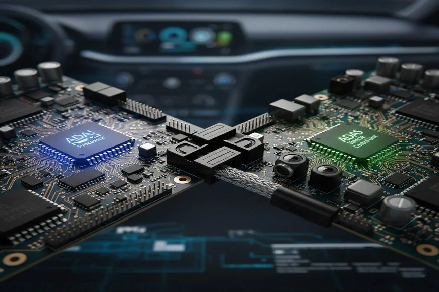
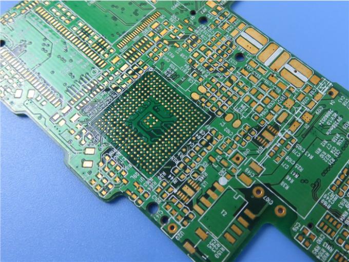
ADAS PCB: The Backbone of Reliable Advanced Driver Assistance Systems

The rapid development of autonomous driving technology has accelerated the adoption of Advanced Driver Assistance Systems (ADAS). These systems integrate radar modules, cameras, LiDAR sensors, and AI computing platforms to enhance driving safety and reduce accidents. Behind these intelligent automotive systems lies a critical hardware component: the ADAS PCB. A well-designed ADAS PCB ensures stable...

Blind Via PCB: Advanced Interconnect Technology for High-Density Multilayer Circuit Boards

As electronic devices become smaller, faster, and more complex, PCB designers must adopt advanced interconnection technologies to achieve higher circuit density. Blind Via PCB technology is widely used in modern HDI PCB designs to enable efficient routing between layers without occupying unnecessary space on the entire board. A Blind Via PCB uses vias that connect...

UAV PCB: High-Reliability Circuit Boards for Unmanned Aerial Vehicle Systems

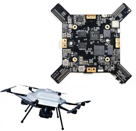
Unmanned Aerial Vehicles (UAVs), commonly known as drones, rely on advanced electronic systems to perform navigation, communication, imaging, and flight control functions. At the core of these systems is the UAV PCB, which integrates critical electronic components to ensure stable operation, lightweight design, and high reliability during flight. UAV PCBs must operate under demanding conditions...

Buried Via PCB: Advanced PCB Design for High-Density and High-Speed Electronics

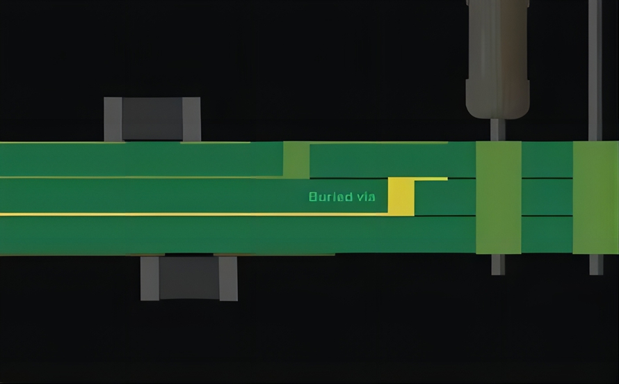
As electronic devices become smaller and more powerful, PCB designers face a constant challenge: fitting more circuitry into less space. Traditional through-hole vias can quickly consume valuable routing area, especially in multilayer boards. This is where Buried Via PCB technology becomes extremely useful. By placing vias entirely within internal layers, designers can maximize routing space...

Microvia PCB: High-Density Interconnect Solutions for Advanced Electronics

Microvia PCB: High-Density Interconnect Solutions for Advanced Electronics As electronic devices become smaller, faster, and more complex, designers face increasing challenges in routing high-density circuits. Microvia PCB technology provides a solution by enabling high-density interconnects (HDI), allowing for compact multilayer designs with superior electrical performance. A Microvia PCB uses extremely small vias, typically less than...

Fine Line PCB: High-Density Circuit Design for Advanced Electronics

Fine Line PCB: High-Density Circuit Design for Advanced Electronics As electronic devices continue to become smaller, faster, and more integrated, traditional PCB manufacturing technologies are often insufficient to meet the demands of modern circuit density. Fine Line PCB technology enables the creation of extremely narrow traces and spaces, allowing engineers to design highly compact and...

HDI PCB: Design, Microvia Technology, and High-Density Applications

High Density Interconnect (HDI) PCB technology is designed to support modern electronic devices that demand higher performance, smaller form factors, and greater circuit complexity. HDI PCBs use advanced manufacturing techniques such as microvias, blind vias, buried vias, and fine line routing to increase the wiring density compared to traditional multilayer PCBs. As electronic products continue...

Buried Via PCB – Advanced Multilayer PCB Technology for High-Density Circuit Design

What Is a Buried Via PCB? A Buried Via PCB is a type of multilayer printed circuit board that uses buried vias to connect internal copper layers without reaching the outer surface layers. Unlike through-hole vias that pass through the entire board, buried vias exist only between inner layers, remaining invisible from the exterior of...

Low Loss PCB – High-Performance PCB for RF and High-Speed Applications

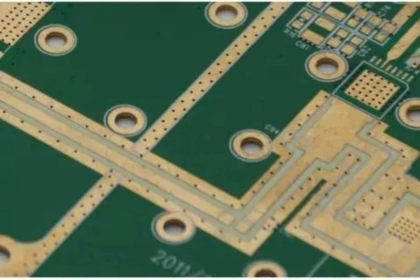
What Is a Low Loss PCB? A Low Loss PCB is a printed circuit board designed with special low-loss dielectric materials to minimize signal attenuation at high frequencies.Unlike standard FR4 boards, low-loss PCBs maintain high signal integrity in RF, microwave, and high-speed digital circuits, making them ideal for: 5G and 6G communication modules Radar systems...