HDI PCB - KKPCB
 
HomeTag

HDI PCB - KKPCB

Microvia PCBs: Design, Reliability, and Engineering Trade-Offs Explained

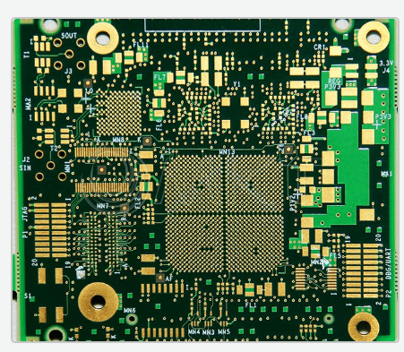
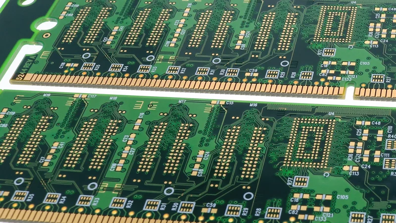
Why Microvias Are Critical in Modern PCB Design As electronic devices continue to shrink while performance demands increase, traditional through-hole vias become a limiting factor. Microvias solve this by enabling high-density interconnects with shorter electrical paths. They are essential when: BGA pitch ≤ 0.8 mm (especially ≤ 0.5 mm) Routing congestion limits layout feasibility High-speed...

HDI PCBs Explained: Stack-Up Choices, Via Strategies, and Cost Trade-Offs

What Actually Defines an HDI PCB? An HDI PCB (High-Density Interconnect PCB) is not defined by layer count alone, but by how efficiently interconnections are implemented. The key differentiators are: Microvias (laser-drilled vias) Blind and buried vias Fine line and spacing (typically ≤100 µm) High connection density per unit area The goal of HDI is...

High Pin Count PCBs: Managing Complexity in Advanced Electronic Systems

System Complexity as the Driving Force Modern electronic systems are no longer defined by individual components, but by highly integrated devices with massive I/O requirements. CPUs, GPUs, FPGAs, and advanced SoCs now feature hundreds to thousands of pins, driving the need for High Pin Count PCBs. This shift introduces a new level of complexity: Multiple...

HDI PCBs: High-Density Interconnect Solutions for Next-Generation Electronics

Why HDI PCBs Are No Longer Optional As electronic devices become smaller, faster, and more complex, traditional multilayer PCB designs struggle to keep up. HDI (High-Density Interconnect) PCBs address this challenge by enabling higher routing density, shorter signal paths, and better electrical performance. At the core of HDI technology is the use of: Microvias (laser-drilled...

High Pin Count PCBs: Enabling Complex Interconnections in Advanced Electronics

Why High Pin Count Matters As modern electronic systems evolve, integrated circuits such as CPUs, GPUs, FPGAs, and high-speed SoCs demand hundreds or even thousands of I/O connections. A High Pin Count PCB is designed to support these devices by enabling dense interconnections within limited board space. Unlike standard PCB designs, high pin count boards...

Buried Via PCBs: Strategic Layer Interconnects for High-Performance Designs

Why Buried Vias Matter As electronic systems become more compact and performance-driven, traditional via structures are no longer sufficient for complex routing requirements. A Buried Via PCB enables connections only between internal layers, eliminating unnecessary vertical paths through the entire board. This design approach is not just about saving space—it is about engineering control over...

Fine Line PCBs: Precision Manufacturing for Ultra-High-Density Electronics

What is a Fine Line PCB? A Fine Line PCB is a printed circuit board designed with extremely narrow trace widths and spacing, typically below 100 microns. These PCBs are essential for high-density electronic designs where space is limited and performance requirements are demanding. Fine line technology is widely used in applications that require compact...

Microvia PCBs: Enabling High-Density and High-Performance Electronics

What is a Microvia PCB? A Microvia PCB is a printed circuit board that uses very small vias—typically less than 150 microns in diameter—to connect adjacent layers. Unlike traditional through-hole or buried vias, microvias enable high-density routing and reduced signal path lengths, making them ideal for high-speed, high-performance, and compact electronic designs. Microvia technology is...

HDI PCBs: Unlocking High-Density Performance for Modern Electronics

High-Density Interconnect (HDI) PCBs are a key technology for today’s compact and high-performance electronics. With fine lines, microvias, blind and buried vias, and multiple layers, HDI PCBs allow designers to fit complex circuits into small form factors, supporting applications from mobile devices to 5G infrastructure, automotive electronics, aerospace systems, and industrial IoT devices. Advanced Design...

ADAS PCB: The Backbone of Reliable Advanced Driver Assistance Systems

The rapid development of autonomous driving technology has accelerated the adoption of Advanced Driver Assistance Systems (ADAS). These systems integrate radar modules, cameras, LiDAR sensors, and AI computing platforms to enhance driving safety and reduce accidents. Behind these intelligent automotive systems lies a critical hardware component: the ADAS PCB. A well-designed ADAS PCB ensures stable...