EMI reduction - KKPCB
 
HomeTag

EMI reduction - KKPCB

Maximize RF Channel Integrity and Minimize Signal Loss with Blind Via PCB Architectures for High-Speed Communication Modules

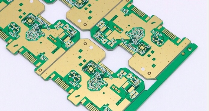
High-speed communication modules in 5G, satellite transceivers, and high-frequency computing systems demand extreme precision in signal routing and interconnect integrity. As layer density increases and modules become more compact, traditional through-hole vias introduce unwanted parasitic effects, signal reflection, and EMI interference, compromising both channel fidelity and system performance. Blind via PCB technology enables selective inter-layer...

Optimizing High-Frequency Stability and Low-Loss Transmission Using RF-35 PCB Laminates for Modern Wireless Systems

RF-35 PCB laminates operate in a class where dielectric precision directly shapes RF linearity, bandwidth uniformity, and system-level efficiency. Modern wireless products—Wi-Fi 6/7 modules, IoT gateways, sub-6 GHz links, and microwave-band transceivers—depend on stable Dk/Df behavior to maintain predictable impedance and low insertion loss. RF-35 offers a low-loss dielectric platform designed for controlled RF propagation,...