HomeTag

Burn-in PCB - KKPCB

IoT IC Test PCB: High-Reliability Test Boards for IoT Chip Validation & Production Testing

What is an IoT IC Test PCB? An IoT IC Test PCB is a specialized test board designed for validating, debugging, and verifying integrated circuits used in IoT devices. Unlike standard PCBs, an IoT IC Test PCB is engineered for repeatable testing, accurate measurement, and long-term reliability. In IoT hardware development, the IoT IC Test...
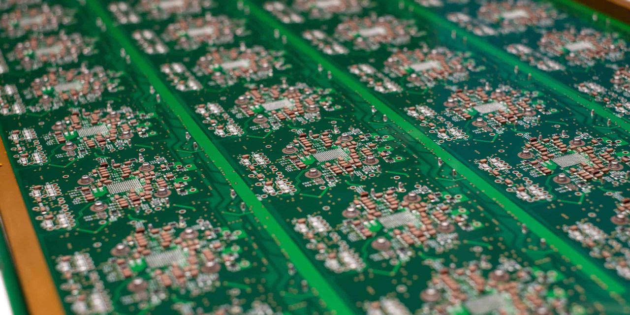
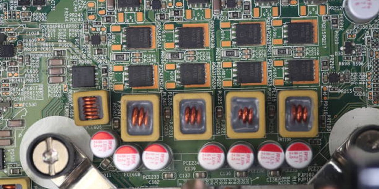
Burn-in PCBs: Ensuring Reliability Through High-Stress Testing

A Burn-in PCB is a printed circuit board specifically designed to support reliability testing of electronic components under elevated temperatures, voltage stress, or operational load. Burn-in testing identifies early-life failures and verifies long-term performance, making these PCBs critical for semiconductor validation, power electronics, and high-reliability systems. Burn-in PCBs are widely used in: Semiconductor testing laboratories...

Burn-in PCB: Ensuring Reliability for High-Performance Electronics

In modern electronics, reliability is key. From industrial control systems to embedded devices and consumer electronics, manufacturers must ensure their products perform consistently over time. One essential tool in this process is the Burn-in PCB, a specialized printed circuit board used for reliability testing under stress conditions . Burn-in testing helps identify early-life failures, verify...

Load Board PCB – High Precision Interface Board for Semiconductor Testing

What Is a Load Board PCB? A Load Board PCB is a critical interface board used in Automated Test Equipment (ATE) systems for semiconductor device testing. It connects the tester to the device under test (DUT), transmitting signals, power, and measurement data with high accuracy and stability. Load boards are specifically engineered to support high...

IoT IC Test PCB – High Precision PCB for IoT Chip Testing Applications

What Is an IoT IC Test PCB? An IoT IC Test PCB is a specialized printed circuit board used for validating and testing integrated circuits (ICs) designed for Internet of Things (IoT) applications. These PCBs are commonly used in semiconductor test environments such as: Automated Test Equipment (ATE) systems Load boards Probe card assemblies Burn-in...

ATE Test PCB – High Precision PCB for Automated Test Equipment Applications

What Is an ATE Test PCB? An ATE Test PCB is a specialized printed circuit board designed for use in Automated Test Equipment (ATE) systems. It acts as the electrical interface between semiconductor devices and the test platform, enabling accurate signal transmission, power delivery, and measurement during IC testing. ATE Test PCB is commonly used...

Burn-in PCB – High Reliability Test Boards for IC Burn-in and Stress Testing

What Is a Burn-in PCB? A Burn-in PCB is a specialized printed circuit board designed for semiconductor burn-in testing. It is used to apply electrical and thermal stress to integrated circuits (ICs) over an extended period to identify early-life failures and ensure long-term reliability. Burn-in testing is a critical quality control process in semiconductor manufacturing,...

Burn-in PCB: High-Reliability PCBs for Burn-In and Stress Testing

What Is a Burn-in PCB? A Burn-in PCB is a specialized printed circuit board used for burn-in testing and stress screening, where electronic components or assemblies are operated under elevated temperature, voltage, and current conditions for extended periods. The goal of a Burn-in PCB is to identify early-life failures and improve long-term product reliability. Burn-in...

Burn-in PCB: Reliable PCBs for Stress Testing and Quality Verification

What Is a Burn-in PCB? A Burn-in PCB is a specialized printed circuit board designed for stress testing and reliability verification of electronic components and assemblies. During burn-in testing, components are subjected to elevated temperatures, voltage, or current to identify early-life failures and ensure long-term reliability. Unlike standard PCBs, Burn-in PCBs must withstand high thermal...

Burn-in PCB Design and Manufacturing for High-Temperature Semiconductor Reliability Testing

A Burn-in PCB is a specialized test interface designed for accelerated semiconductor reliability screening under sustained electrical and thermal stress. In burn-in systems, the PCB is exposed to continuous high temperature, elevated voltage, and long operating cycles, making it one of the most mechanically and electrically stressed PCB types in semiconductor test environments. Unlike functional...