HomeTag

RF PCB - KKPCB

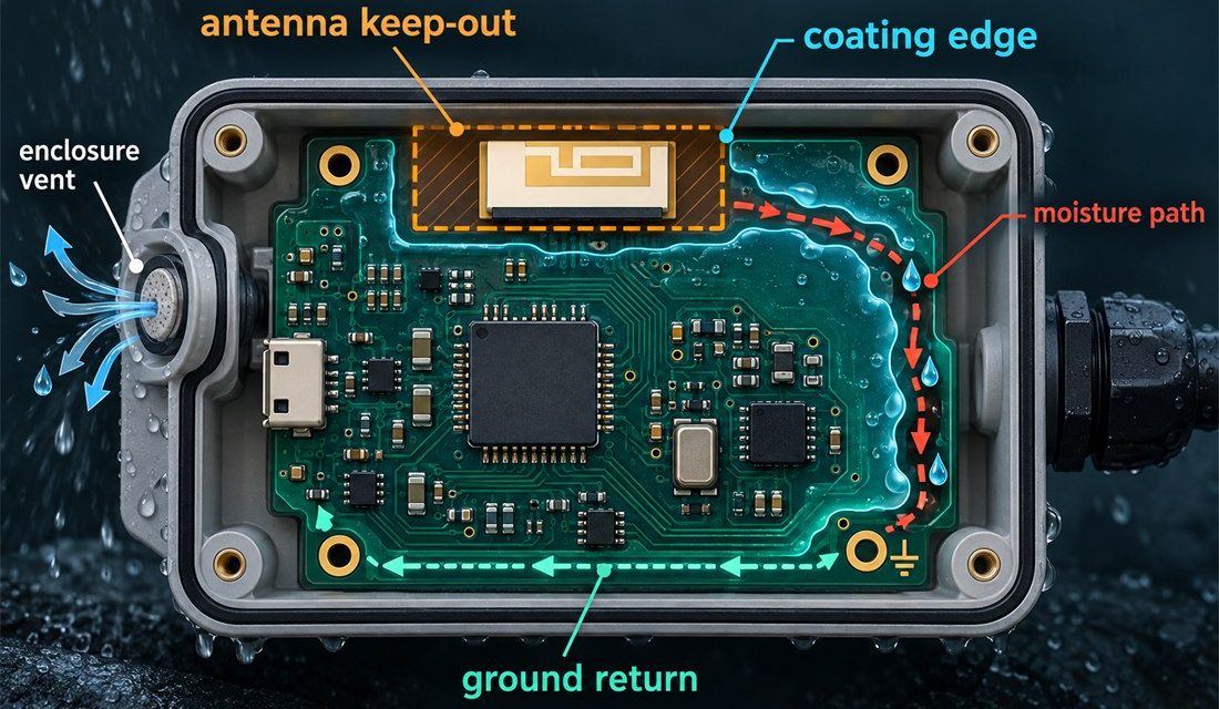
When a LoRa PCB Range Test Changes After Conformal Coating

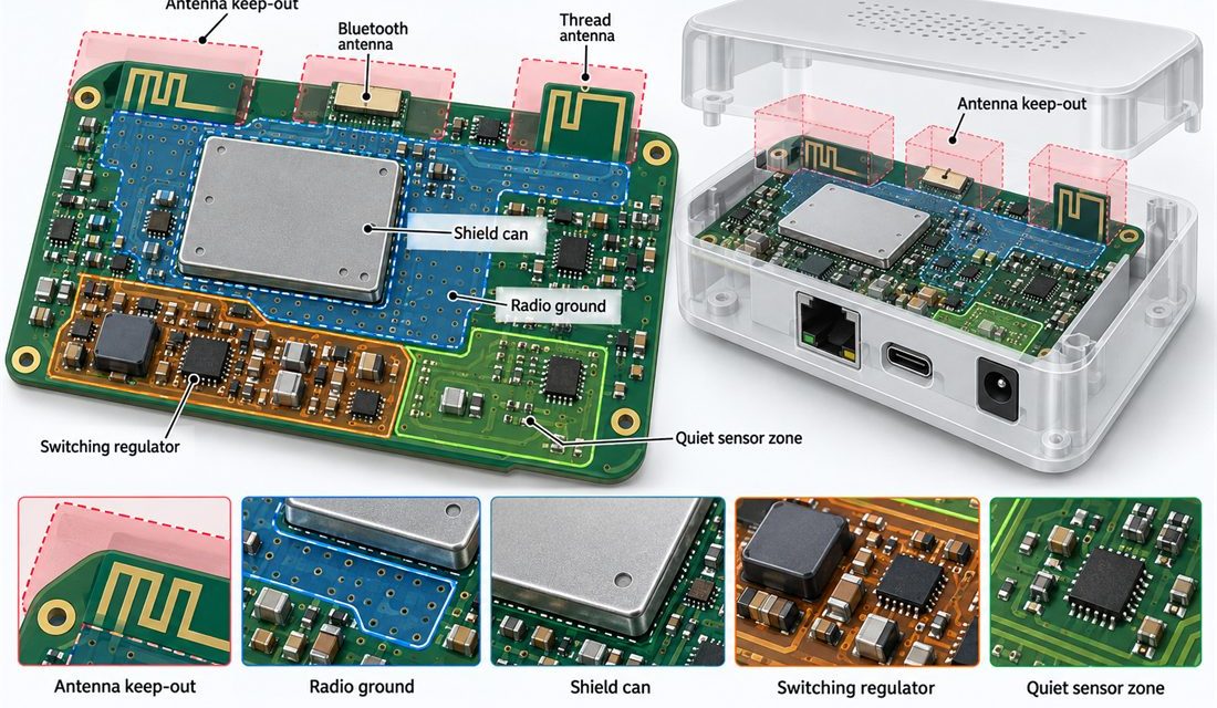
Table of Contents Why coating can change a range result Protect the antenna boundary before coating Control cleaning, masking, and cure Verify the coated assembly without false comparisons A release checklist for environmental builds A LoRa PCB can meet its bench range target and then behave differently after conformal coating, cleaning, or enclosure sealing. The...

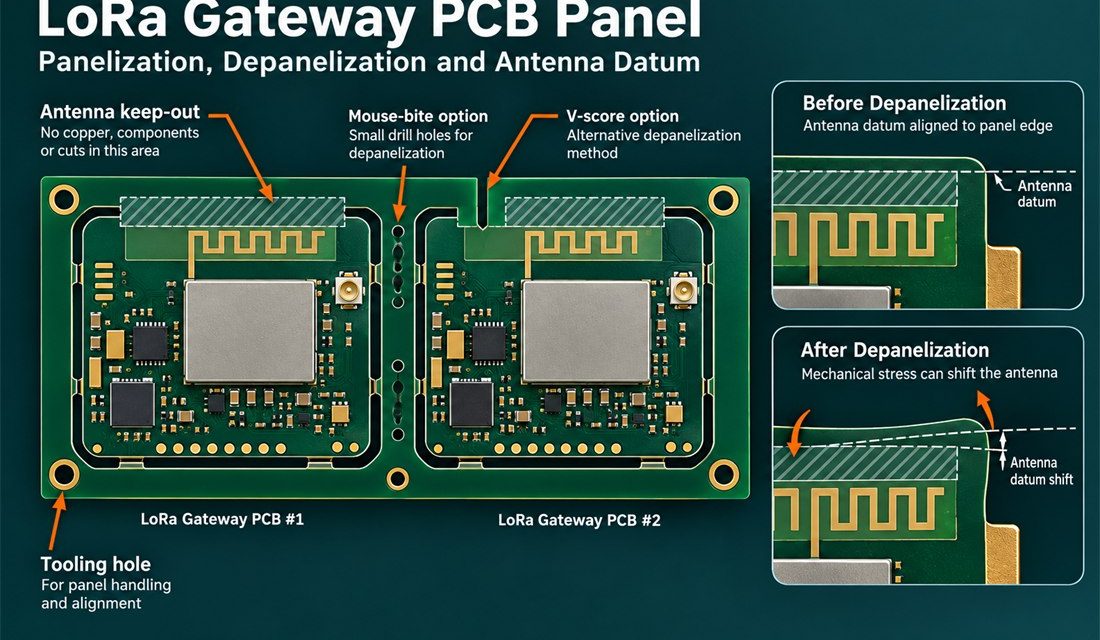
What the Assembly Line Can Change on a Radar PCB

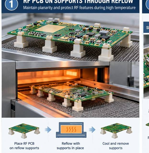
Radar PCB assembly release begins by treating heat, solder, cleaning, and mechanical force as RF variables. An RF board can leave fabrication within drawing limits and still change during paste printing, reflow, shielding, cleaning, or mechanical assembly. That risk is amplified in short-range and imaging radar front ends where antenna phase error, launch repeatability, and...

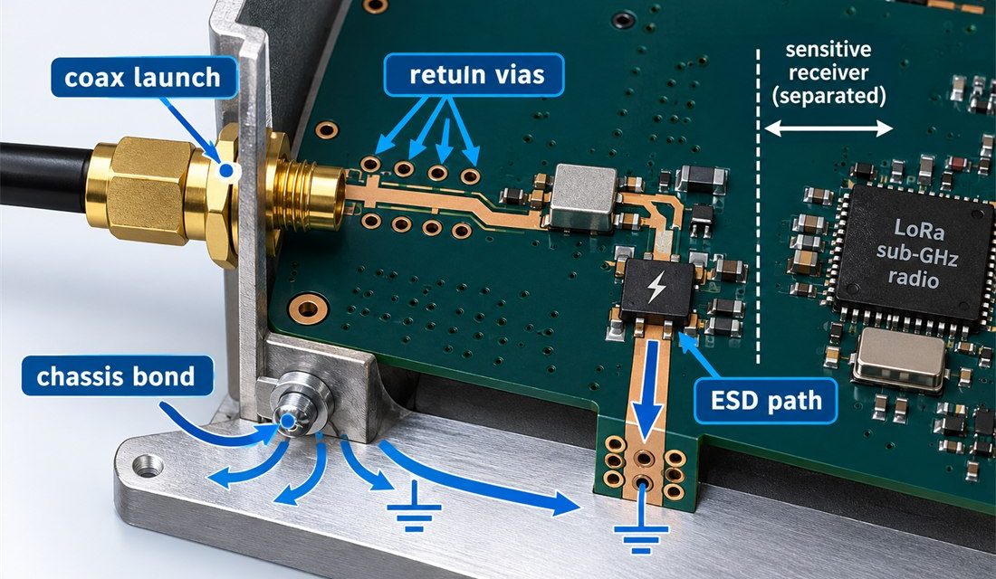
A Ground-Return Strategy for Radar PCB Antenna Transitions

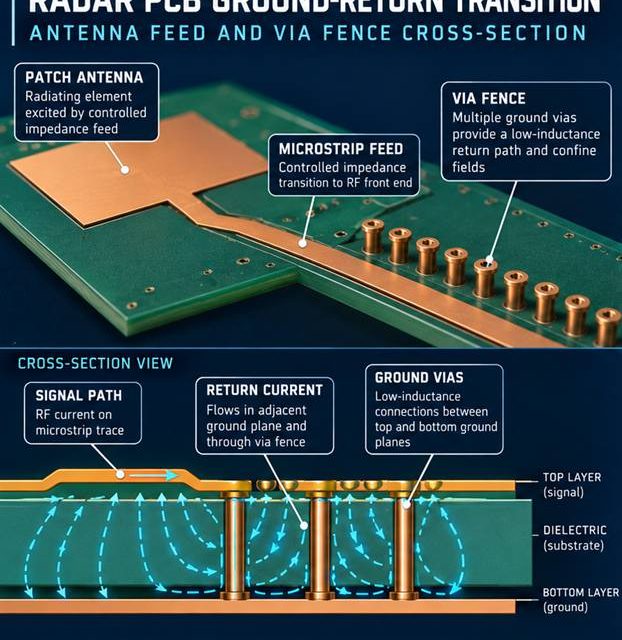
Radar PCB launch design begins with a complete three-dimensional signal and return path. The boundary between a board and a connector, coax, antenna, or shield is where a clean schematic becomes a three-dimensional electromagnetic problem. In short-range and imaging radar front ends where antenna phase error, launch repeatability, and thermal drift all affect detection margin,...

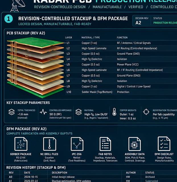
How a Radar PCB Stackup Preserves Phase Consistency Across the Array

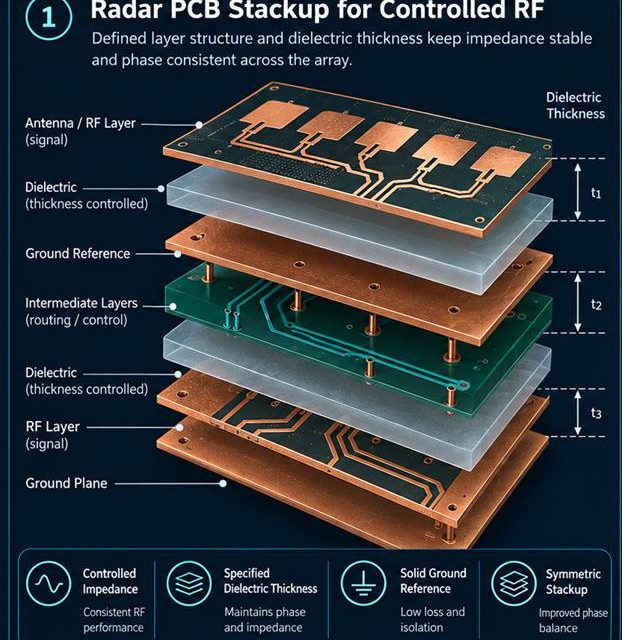
Radar PCB stackup release begins by making every electromagnetic and manufacturing assumption visible. Stackup discussions fail when the drawing lists layer names but not the electromagnetic and manufacturing assumptions behind them. In short-range and imaging radar front ends where antenna phase error, launch repeatability, and thermal drift all affect detection margin, the board must carry...