HomeCategory

PCB Manufacturing Services | High-Quality PCB & PCBA - KKPCB

Protecting RF Geometry During Automotive Radar PCB Assembly

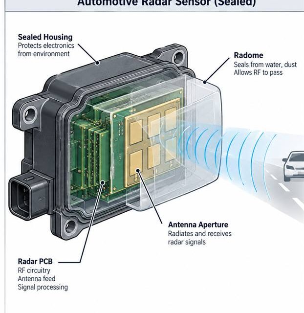
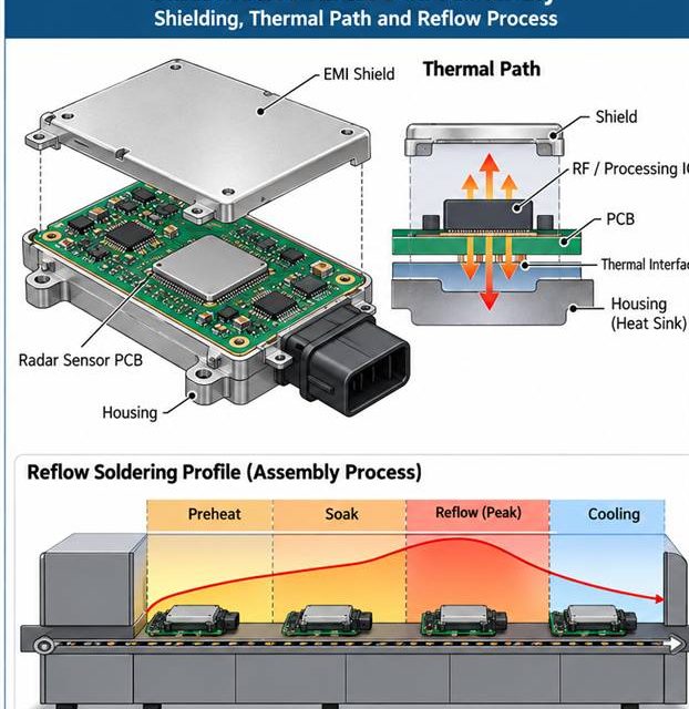
Automotive Radar PCB assembly release begins by treating heat, solder, cleaning, and mechanical force as RF variables. An RF board can leave fabrication within drawing limits and still change during paste printing, reflow, shielding, cleaning, or mechanical assembly. That risk is amplified in front and corner radar sensors exposed to vibration, temperature cycling, radome constraints,...
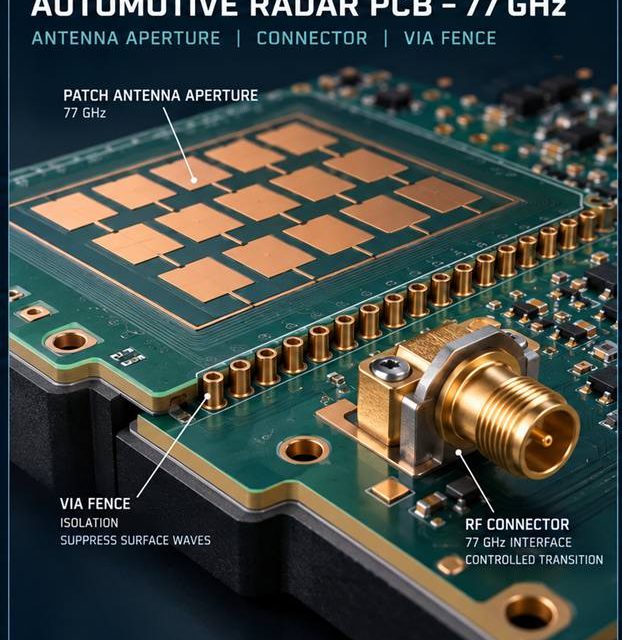
Controlling the 77 GHz Launch on an Automotive Radar PCB

Automotive Radar PCB launch design begins with a complete three-dimensional signal and return path. The boundary between a board and a connector, coax, antenna, or shield is where a clean schematic becomes a three-dimensional electromagnetic problem. In front and corner radar sensors exposed to vibration, temperature cycling, radome constraints, and strict end-of-line calibration, that boundary...

Building an Automotive Radar PCB Stackup That Survives Thermal History

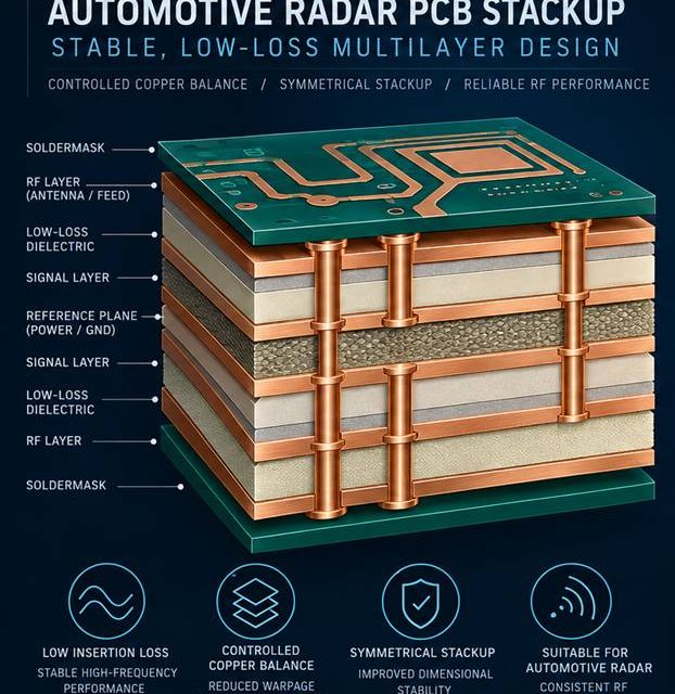
Automotive Radar PCB stackup release begins by making every electromagnetic and manufacturing assumption visible. Stackup discussions fail when the drawing lists layer names but not the electromagnetic and manufacturing assumptions behind them. In front and corner radar sensors exposed to vibration, temperature cycling, radome constraints, and strict end-of-line calibration, the board must carry RF energy,...

Finding the Root Cause of Drift in an Automotive Radar PCB

Automotive Radar PCB fault isolation begins at the physical boundary where the symptom is reproduced. A front and corner radar sensors exposed to vibration, temperature cycling, radome constraints, and strict end-of-line calibration can pass a schematic review and still fail in the chamber, the enclosure, or the vehicle. The failure often appears as a receiver...

A Thermal-and-Soldering Plan for Reliable 5G Router PCB Assembly

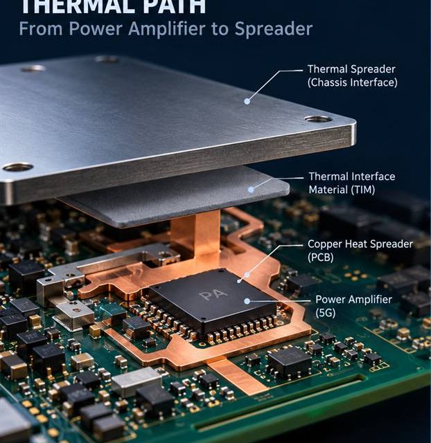
5G router PCB assembly release begins by treating heat, solder, cleaning, and mechanical force as RF variables. An RF board can leave fabrication within drawing limits and still change during paste printing, reflow, shielding, cleaning, or mechanical assembly. That risk is amplified in indoor and outdoor 5G routers that combine cellular radios, Ethernet switching, Wi-Fi,...

Where 5G Router PCB Antenna Feeds Lose Margin at the Enclosure Boundary

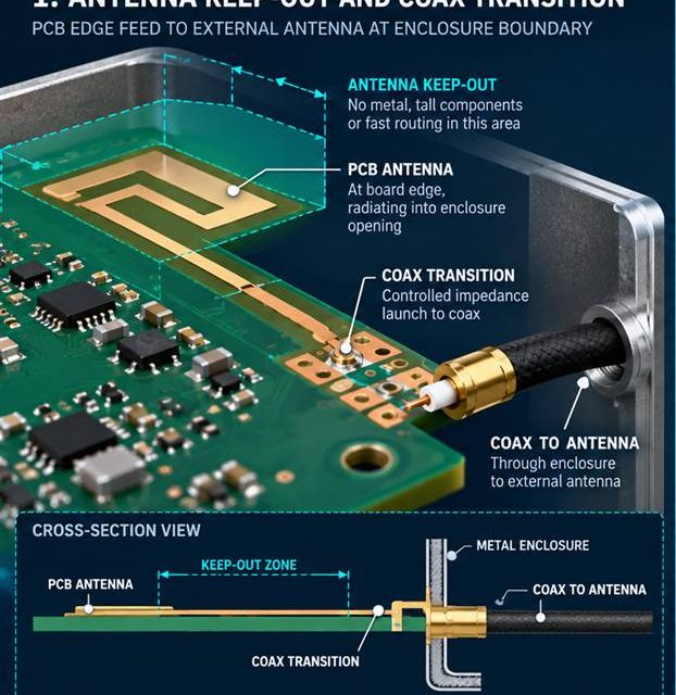
5G router PCB launch design begins with a complete three-dimensional signal and return path. The boundary between a board and a connector, coax, antenna, or shield is where a clean schematic becomes a three-dimensional electromagnetic problem. In indoor and outdoor 5G routers that combine cellular radios, Ethernet switching, Wi-Fi, and a metal enclosure, that boundary...

A Release Method for 5G Router PCB Stackups Under Mixed-Signal Constraints

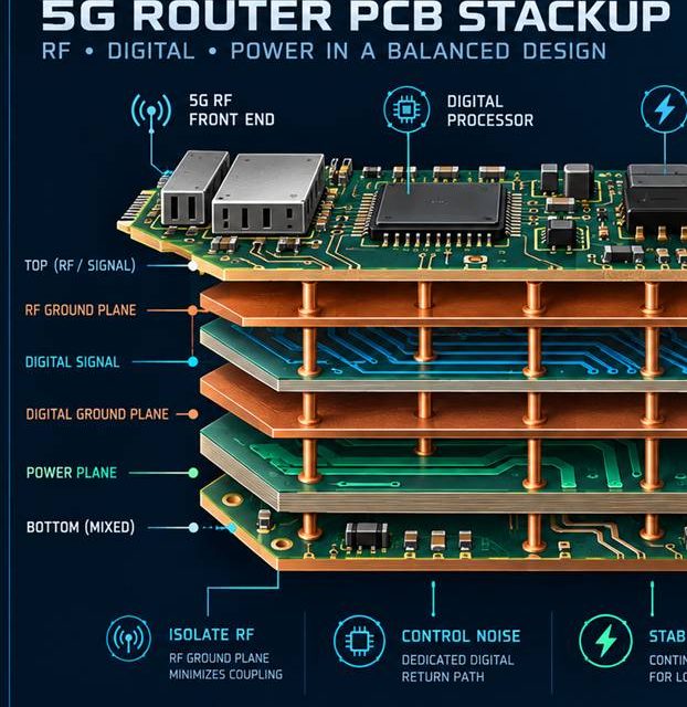
5G router PCB stackup release begins by making every electromagnetic and manufacturing assumption visible. Stackup discussions fail when the drawing lists layer names but not the electromagnetic and manufacturing assumptions behind them. In indoor and outdoor 5G routers that combine cellular radios, Ethernet switching, Wi-Fi, and a metal enclosure, the board must carry RF energy,...

Stabilizing a 5G Router PCB When Mixed-Signal Traffic Becomes Unpredictable

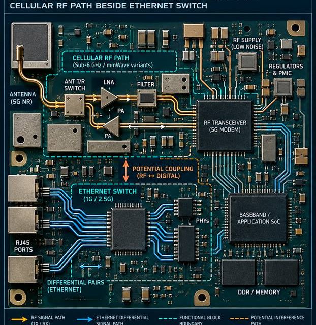
5G router PCB fault isolation begins at the physical boundary where the symptom is reproduced. A indoor and outdoor 5G routers that combine cellular radios, Ethernet switching, Wi-Fi, and a metal enclosure can pass a schematic review and still fail in the chamber, the enclosure, or the vehicle. The failure often appears as a receiver...

From EVT Evidence to Volume Release for a 5G Module PCB

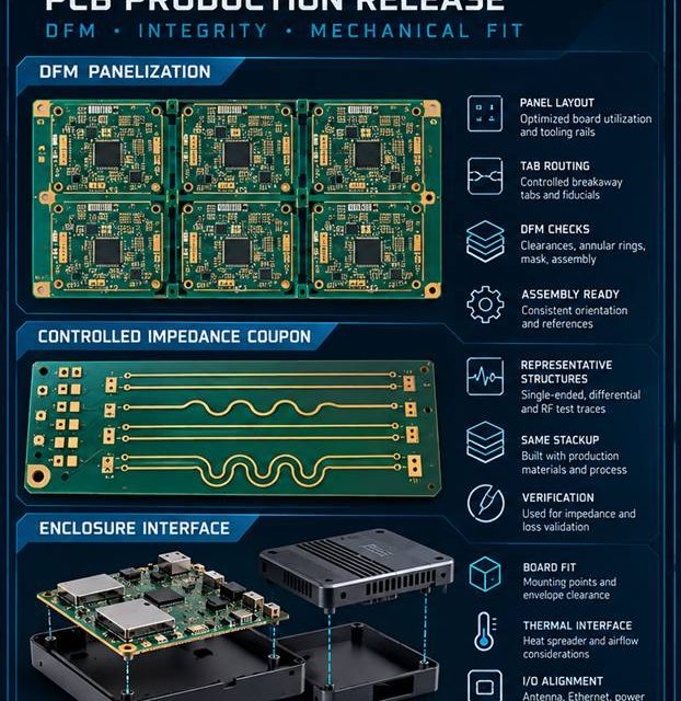
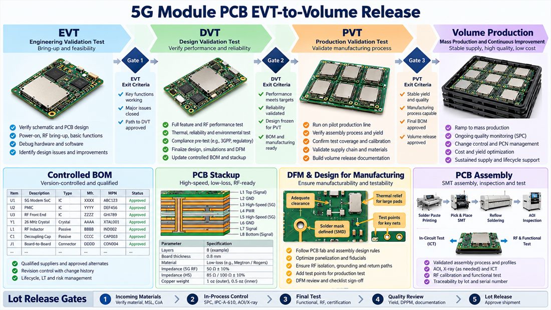
5G module PCB production release begins when design evidence, supplier capability, and change control agree. The last ten percent of a board program is rarely a single design change. It is the point where a prototype stackup, a supplier process, a connector choice, and an enclosure must become one controlled release. For compact radio modules...