PCB Manufacturing Services | High-Quality PCB & PCBA - KKPCB
 
HomeCategory

PCB Manufacturing Services | High-Quality PCB & PCBA - KKPCB

HDI Printed Circuit Board (PCB)

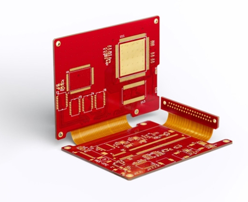
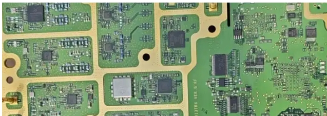
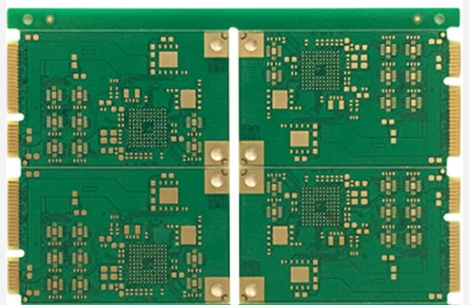
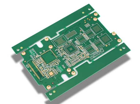
What’s HDI PCB? High-density interconnect (HDI) PCBs are characterized by finer lines, closer spaces, and more dense wiring, which allow for a faster connection while reducing the size and bulk of a project. These boards also feature blind and buried vias, laser ablated microvias, sequential lamination, and via in-pads. As a result, a HDI board can house the functionality of the previous...

What Are Flexible Printed Circuits (Flex PCB)?

Flexible Printed Circuits (FPCs), also called Flexible Circuits, or Flex Circuits, by IPC definition, a flexible printed circuit is a patterned arrangement of printed circuitry and components that utilizes flexible based material with or without flexible cover lay. This definition is accurate, and conveys some of the potential given the available variations in base materials, conductor materials, and protective cover materials....

PCB Prototyping Services

In modern electronics development, PCB prototyping services play a critical role in transforming circuit concepts into functional hardware. Whether for high-speed PCB design, RF PCB development, or industrial electronics, fast and accurate PCB prototype manufacturing ensures design validation, reduces risks, and accelerates time-to-market. Professional PCB prototyping services provide engineers with rapid turnaround, high-quality fabrication, and...

Common Flex PCB Surface Finishes

Copper in Printed Circuit Boards Printed circuit boards (PCBs), or called printed wiring boards (PWBs), have become basic parts in almost all areas of modern technologies. Copper trace is a crucial element on circuit boards. The copper always plays a role of carrying electrical signals to different components across the board assembly. Without traces, the...

Multilayer PCB Benefits and Applications

Printed circuit boards (PCBs) are the core of most electronics today, determining basic functions through combinations of components and wiring mechanisms. Most PCBs of the past were relatively simple and limited by manufacturing techniques, while today’s PCBs are much more complex. From advanced flexible options to odd-shaped varieties, PCBs are much more varied in nowadays’ world...

What is Stack-up?

Stack-up refers to the arrangement of copper layers and insulating layers that make up a PCB prior to board layout design. While a layer stack-up allows you to get more circuitry on a single board through the various PCB board layers, the structure of PCB stackup design confers many other advantages: • A PCB layer stack...

Blind Via and Buried Via

In modern PCB design, Blind Via and Buried Via technologies play a critical role in achieving high-density interconnect (HDI) structures, improving signal integrity, and optimizing PCB layout performance. As electronic devices continue to evolve toward miniaturization, high speed, and high functionality, the use of blind vias and buried vias has become increasingly essential in advanced...

Advantages and Disadvantages of Multilayer PCBs

Multilayer PCBs (Printed Circuit Boards) are integral to modern electronics, offering unparalleled performance in compact designs. While they come with several benefits, they also present unique challenges. This article delves into the advantages and disadvantages of multilayer PCBs, providing insight into their role in electronic design and manufacturing. Advantages of Multilayer PCBs 1. Higher Density and Efficiency...

Multilayer PCB: What It Is, How It Works, and When to Use It

In the evolution of printed circuit boards (PCBs), the transition from single-sided to double-sided to multilayer PCBs has been pivotal. This shift addresses the growing demand for compact, efficient, and high-performance electronic devices. Here’s a detailed look at what multilayer PCBs are, how they work, and when to use them. What Is a Multilayer PCB? A multilayer PCB is an advanced circuit board featuring multiple layers of...