
In PCB design and manufacturing, stack-up is one of the most important elements that determines the electrical performance, mechanical reliability, and manufacturability of a printed circuit board.
As electronic products continue to develop toward:
- Higher transmission speeds
- Smaller form factors
- Greater circuit density
- More complex power requirements
PCB layer arrangement has become increasingly critical. A well-designed stack-up helps control:
- Signal integrity
- Power integrity
- Electromagnetic interference (EMI)
- Thermal performance
- Manufacturing stability
Whether designing a simple multilayer PCB or an advanced high-speed board, the stack-up should be considered early in the design process.
1. What Is PCB Stack-Up?
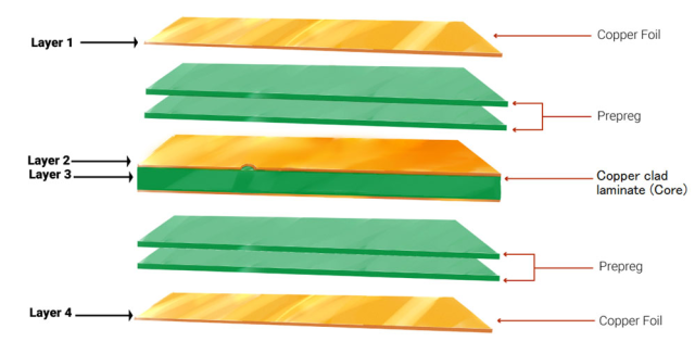
A PCB stack-up refers to the arrangement and sequence of different material layers that make up a multilayer printed circuit board.
A typical PCB stack-up consists of:
- Copper layers
- Dielectric layers
- Core materials
- Prepreg materials
- Solder mask layers
- Surface finish layers
The stack-up defines how these layers are positioned relative to each other.
For example, a simple 4-layer PCB stack-up may be arranged as:
| Layer | Function |
|---|---|
| Top Layer | Component placement and signal routing |
| Inner Layer 1 | Ground plane |
| Inner Layer 2 | Power plane |
| Bottom Layer | Signal routing |
A more complex PCB may contain:
- 6 layers
- 8 layers
- 10+ layers
- HDI structures with microvias
depending on design requirements.
2. Main Components of a PCB Stack-Up
2.1 Copper Layers
Copper layers provide electrical connections.
They are used for:
- Signal routing
- Power distribution
- Ground connections
Copper thickness affects:
- Current carrying capability
- Impedance
- Manufacturing capability
Common copper thickness options include:
- 0.5 oz
- 1 oz
- 2 oz
- Heavy copper structures
2.2 Core Material
The core is a rigid dielectric material with copper foil bonded on both sides.
Common core materials include:
- FR-4
- High-Tg FR-4
- Low-loss laminates
- RF materials
The core provides:
- Mechanical strength
- Electrical insulation
- Dimensional stability
2.3 Prepreg
Prepreg is a layer of fiberglass material impregnated with partially cured resin.
During lamination, the resin melts and bonds PCB layers together.
Prepreg thickness influences:
- Layer spacing
- Impedance control
- Overall board thickness
2.4 Dielectric Layer
The dielectric layer separates conductive layers.
Important parameters include:
Dielectric Constant (Dk)
Affects:
- Signal propagation speed
- Impedance calculation
Dissipation Factor (Df)
Affects:
- Signal loss
- High-frequency performance
Low-loss materials are commonly used for:
- RF circuits
- 5G systems
- High-speed communication boards
3. Why Is PCB Stack-Up Important?
3.1 Signal Integrity Control
For high-speed PCB designs, signals travel as electromagnetic waves rather than simple electrical currents.
Poor stack-up design may cause:
- Signal reflection
- Crosstalk
- Increased insertion loss
A proper stack-up provides:
- Controlled impedance
- Stable return paths
- Reduced noise
3.2 Impedance Control
PCB traces have a characteristic impedance determined by:
- Trace width
- Copper thickness
- Dielectric thickness
- Material properties
Common impedance requirements include:
- 50 Ω single-ended signals
- 90 Ω differential pairs
- 100 Ω differential pairs
The PCB stack-up must be designed together with routing requirements.
3.3 Power Integrity Improvement
Power and ground layers form the power distribution network (PDN).
A good stack-up helps:
- Reduce voltage fluctuations
- Minimize power noise
- Improve current return paths
This is especially important for:
- CPUs
- FPGAs
- Power converters
- Communication modules
3.4 EMI and EMC Performance
A well-designed stack-up reduces electromagnetic interference.
Benefits include:
- Better shielding
- Reduced radiation
- Improved noise immunity
Placing signal layers close to reference planes helps contain electromagnetic fields.
3.5 Mechanical Reliability
Stack-up design also affects:
- PCB thickness
- Warpage
- Layer balance
- Thermal expansion
Balanced layer distribution helps prevent:
- Board bending
- Lamination stress
- Reliability problems
4. Common PCB Stack-Up Structures
4.1 2-Layer PCB Stack-Up
Structure:
| Layer | Function |
|---|---|
| Top Copper | Signal routing |
| Dielectric Core | Insulation |
| Bottom Copper | Signal routing |
Advantages:
- Low cost
- Simple manufacturing
Applications:
- Simple controllers
- Consumer electronics
- Basic industrial products
4.2 4-Layer PCB Stack-Up
Common structure:
| Layer | Function |
|---|---|
| L1 | Signal |
| L2 | Ground |
| L3 | Power |
| L4 | Signal |
Advantages:
- Better signal integrity
- Improved power distribution
Applications:
- Industrial electronics
- Embedded systems
- Communication products
4.3 6-Layer PCB Stack-Up
Example:
| Layer | Function |
|---|---|
| L1 | Signal |
| L2 | Ground |
| L3 | Signal |
| L4 | Signal |
| L5 | Power |
| L6 | Signal |
Advantages:
- More routing space
- Better high-speed performance
Applications:
- High-speed digital systems
- Automation equipment
- Communication devices
4.4 HDI Stack-Up
HDI PCB stack-ups use:
- Microvias
- Sequential lamination
- Fine-line routing
Common structures:
- 1+N+1
- 2+N+2
- Any-layer HDI
Advantages:
- Higher density
- Smaller form factor
- Better electrical performance
Applications:
- Smartphones
- Wearable devices
- Advanced electronic modules
5. Factors to Consider When Designing PCB Stack-Up
5.1 Signal Requirements
Consider:
- Signal frequency
- Data rate
- Interface type
High-speed signals may require:
- Dedicated routing layers
- Adjacent reference planes
- Controlled impedance
5.2 Power Requirements
Consider:
- Voltage levels
- Current requirements
- Noise sensitivity
Power-intensive designs may need:
- Dedicated power planes
- Thick copper layers
- Thermal solutions
5.3 PCB Thickness Requirements
The final thickness depends on:
- Number of layers
- Material selection
- Mechanical requirements
Common PCB thicknesses include:
- 0.8 mm
- 1.0 mm
- 1.6 mm
- Custom thickness options
5.4 Material Selection
Different applications require different materials.
FR-4
Suitable for:
- General electronics
- Industrial control boards
High-Tg Materials
Suitable for:
- High-temperature environments
- Automotive electronics
Low-Loss Materials
Suitable for:
- RF PCB
- Microwave circuits
- High-speed communication
6. PCB Stack-Up and Manufacturing Process
A stack-up must be compatible with PCB manufacturing capabilities.
Important manufacturing factors include:
Lamination Control
Precise control is needed for:
- Temperature
- Pressure
- Layer alignment
Drilling and Via Technology
Stack-up affects:
- Through vias
- Blind vias
- Buried vias
- Microvias
Impedance Verification
Manufacturers may use:
- TDR testing
- Cross-section analysis
to verify impedance performance.
7. Common PCB Stack-Up Design Mistakes
7.1 Incorrect Reference Plane Arrangement
Poor placement of ground planes can cause:
- Increased EMI
- Signal integrity problems
7.2 Excessive Layer Changes
Frequent layer transitions increase:
- Via inductance
- Signal discontinuity
7.3 Unbalanced Layer Structure
Uneven copper distribution may cause:
- PCB warpage
- Manufacturing issues
7.4 Ignoring Manufacturing Capability
A theoretically optimized stack-up may be difficult to manufacture.
Consider:
- Minimum dielectric thickness
- Via capability
- Material availability
- Production tolerance
8. Importance of DFM Review for Stack-Up Design
Before PCB production, a DFM review helps confirm:
- Stack-up feasibility
- Material compatibility
- Impedance requirements
- Manufacturing tolerance
A professional PCB manufacturer can assist with:
- Layer planning
- Material selection
- Signal integrity considerations
- Production optimization
Conclusion
PCB stack-up is the foundation of multilayer PCB design. It determines how copper layers, dielectric materials, and signal paths interact to achieve reliable electrical and mechanical performance.
A well-designed stack-up helps improve:
- Signal integrity
- Power distribution
- EMI/EMC performance
- Thermal reliability
- Manufacturing consistency
As electronic products continue moving toward higher speeds and greater integration, proper PCB stack-up planning becomes increasingly important for applications such as communication equipment, automotive electronics, industrial control systems, RF systems, and advanced computing platforms.
By considering electrical requirements, material characteristics, and manufacturing capabilities during the design stage, engineers can create PCBs with improved performance and long-term reliability.
